APJ ABDUL KALAM TECHNOLOGICAL UNIVERSITY Previous Years Question Paper & Answer
Semester : SEMESTER 3
Subject : Logic Circuit Design
Year : 2017
Term : JULY
Scheme : 2015 Full Time
Course Code : EC 207
Page:2
B3E011S Pages: 3
b) Draw the circuit diagram of a transistor level TTL NAND gate and explain the
working. (5)
€) What is PLDs?. Differentiate between PAL and PLA. (4)
+ a) Realize a JK flip flop with NAND gates and describe its operation with detailed
truth table, characteristic equation and excitation table. Describe the race around
problem and suggest the methods to eliminate. (5)
b) A self starting synchronous binary up-counter having the state sequence 1; 2; 3; 4;
5; 6; 1; 2; : : : is to be implemented using T-flip flops. The flip flop outputs are
designated as Qo, ಛಿ; and Qo, where Qo represents the least significant digit of the
count. Give simplified expressions for the required next-state logic and the complete
circuit diagram. (10)
. a) Draw the circuit diagram of a transistor level CMOS NOR gate and explain the
working with a truth table. (4)
b) Differentiate between the totem pole, open collector and tri-state logic related to
the TTL logic circuit. (3)
€) Describe the procedure for converting one type of flip flop in to another. Perform
the following conversions. (8)
i) T toJK ii) TtoD
PART C
Answer two questions, Question no. 9 is compulsory.
+ a) Draw the logic diagram of a four bit Johnson counter and explain the working with
truth table and timing diagram. (10)
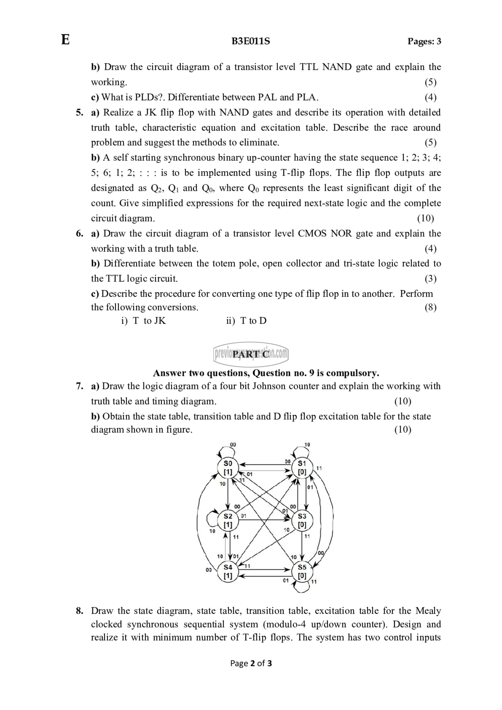
b) Obtain the state table, transition table and D flip flop excitation table for the state
diagram shown in figure. (10)
. Draw the state diagram, state table, transition table, excitation table for the Mealy
clocked synchronous sequential system (modulo-4 up/down counter). Design and
realize it with minimum number of T-flip flops. The system has two control inputs
Page 2 of 3
