APJ ABDUL KALAM TECHNOLOGICAL UNIVERSITY Previous Years Question Paper & Answer
Semester : SEMESTER 3
Subject : Logic Circuit Design
Year : 2017
Term : JULY
Scheme : 2015 Full Time
Course Code : EC 207
Page:3
B3E011S Pages: 3
and two outputs: input (mode) M is set at logic "“0'' (௦ cause the counter to count up,
and at logic "“1'' to cause the counter to count down; input (enable) E is set at logic “1"
to enable the counter to count and at logic “0" to cause the counter to hold its current
state. The outputs “Y,Z” become “00”, “017, “10 ஹம் “11” in count up direction
and output “Y,Z” become “11”, “10”, “017 वात “00” in countdown direction against
the clock starting from the first state. (20)
+ a) Draw the logic diagram of a four bit, bi-directional serial in serial out (SISO) shift
register with mode control and explain the working with timing diagram.
(10)
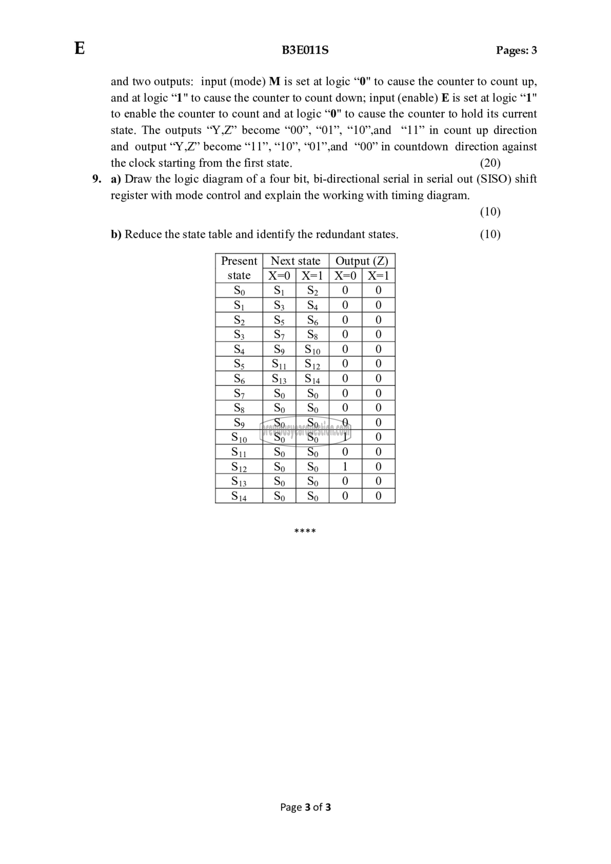
b) Reduce the state table and identify the redundant states. (10)
@ | > |- | ॐ
KKK
Page 3 of 3
