APJ ABDUL KALAM TECHNOLOGICAL UNIVERSITY Previous Years Question Paper & Answer
Semester : SEMESTER 6
Subject : VLSI
Year : 2019
Term : MAY
Scheme : 2015 Full Time
Course Code : EC 304
Page:1
Reg No.:_. Name:
Max. Marks: 100
1 a)
b)
2 a)
b)
3 a)
b)
4 a)
b)
5 ஐ
b)
6 a)
b)
7 a)
b)
8 a)
b)
9 a)
F1034 Pages: 2
APJ ABDUL KALAM TECHNOLOGICAL UNIVERSITY
SIXTH SEMESTER B.TECH DEGREE EXAMINATION(R&S), MAY 2019
Course Code: EC304
Course Name: VLSI
PARTA
Answer any two full questions, each carries 15 marks
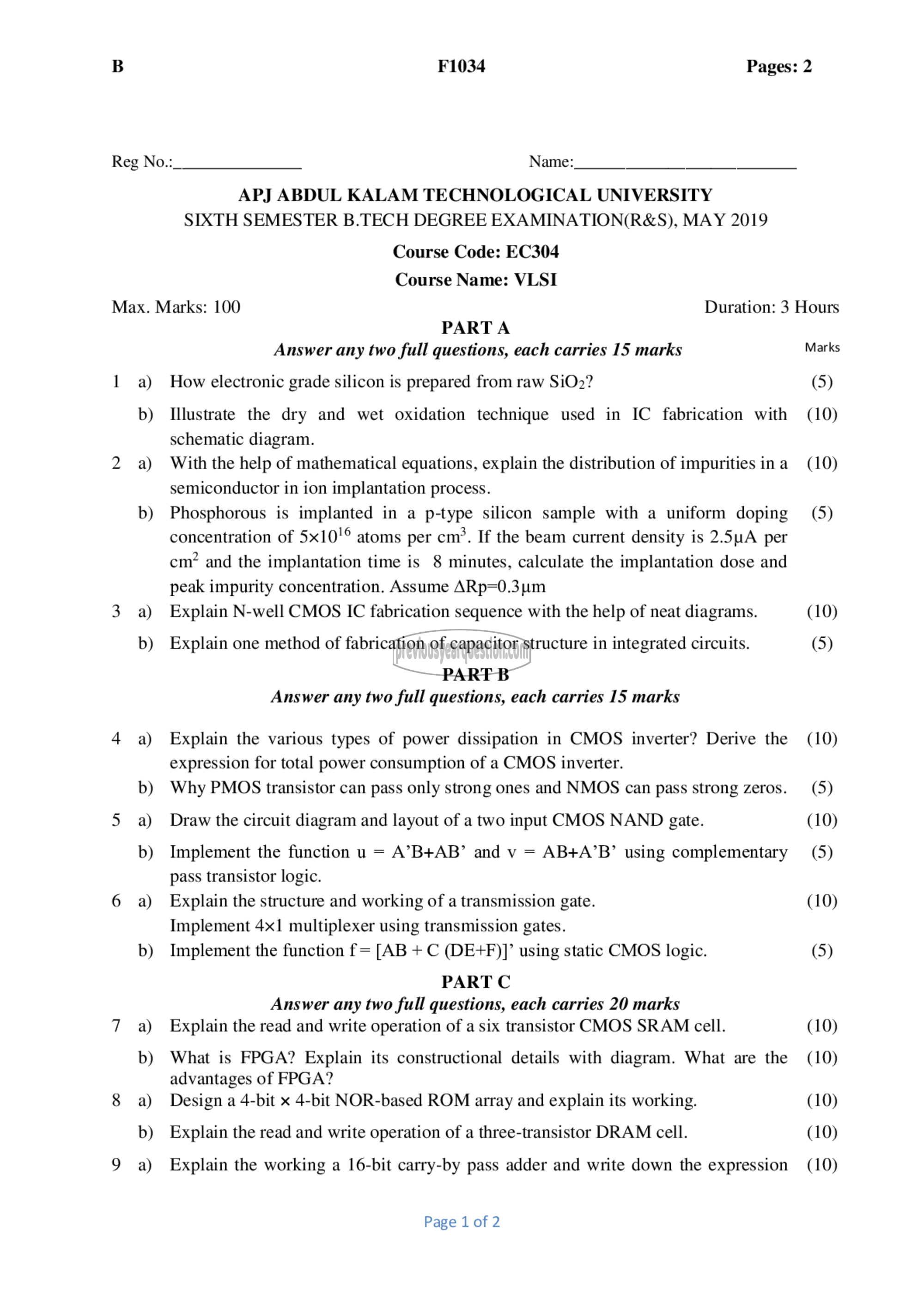
How electronic grade silicon is prepared from raw SiO2?
Illustrate the dry and wet oxidation technique used in IC fabrication with
schematic diagram.
With the help of mathematical equations, explain the distribution of impurities in a
semiconductor in ion implantation process.
Phosphorous is implanted in a p-type silicon sample with a uniform doping
concentration of 5x10!° atoms per cm’. If the beam current density is 2.5uA per
cm’ and the implantation time is 8 minutes, calculate the implantation dose and
peak impurity concentration. Assume ARp=0.3 um
Explain N-well CMOS IC fabrication sequence with the help of neat diagrams.
Explain one method of fabrication of capacitor structure in integrated circuits.
PART B
Answer any two full questions, each carries 15 marks
Explain the various types of power dissipation in CMOS inverter? Derive the
expression for total power consumption of a CMOS inverter.
Why PMOS transistor can pass only strong ones and NMOS can pass strong zeros.
Draw the circuit diagram and layout of a two input CMOS NAND gate.
Implement the function प्र = A’B+AB’ and v = AB+A’B’ using complementary
pass transistor logic.
Explain the structure and working of a transmission gate.
Implement 4x1 multiplexer using transmission gates.
Implement the function f= [AB + C (DE+F)]’ using static CMOS logic.
PART ட
Answer any two full questions, each carries 20 marks
Explain the read and write operation of a six transistor CMOS SRAM cell.
What is FPGA? Explain its constructional details with diagram. What are the
advantages of FPGA?
Design a 4-bit x 4-bit NOR-based ROM array and explain its working.
Explain the read and write operation of a three-transistor DRAM cell.
Explain the working a 16-bit carry-by pass adder and write down the expression
Page 1 of 2
Duration: 3 Hours
Marks
(5)
(10)
(10)
(5)
(10)
(5)
(10)
(5)
(10)
(5)
(10)
(5)
(10)
(10)
(10)
(10)
(10)
