APJ ABDUL KALAM TECHNOLOGICAL UNIVERSITY Previous Years Question Paper & Answer
Semester : SEMESTER 6
Subject : VLSI
Year : 2019
Term : DECEMBER
Scheme : 2015 Full Time
Course Code : EC 304
Page:1
B F192022 Pages:2
Reg No.:_ Name:
APJ ABDUL KALAM TECHNOLOGICAL UNIVERSITY
SIXTH SEMESTER B.TECH DEGREE EXAMINATION(S), DECEMBER 2019
Course Code: EC304
Course Name: VLSI
Max. Marks: 100 Duration: 3 Hours
PARTA
Answer any two full questions, each carries 15 marks Marks
1 a) With a neat sketch, explain the process of ion implantation for IC fabrication. (8)
b) Draw schematic and explain any two CVD processes. (7)
2 a) With the help of neat diagram explain crystal growth in Czochralski process. (7)
b) Define photolithography and discuss various steps involved in photolithographic (8)
process.
3 a) A Si sample is covered with 0.25um thick SiO, layer. Find the time required to (5)
grow an additional 0.2um thick 5702 at 12001) by dry oxidation. For dry
oxidation at 12000 B=0.045 um, B/A = 1.120 um/hr, t = 0.027
b) Solve Fick’s law for pre deposition diffusion. (3)
c) List various methods of resistor fabrication. (7)
PART छ
Answer any two full questions, each carries 15 marks
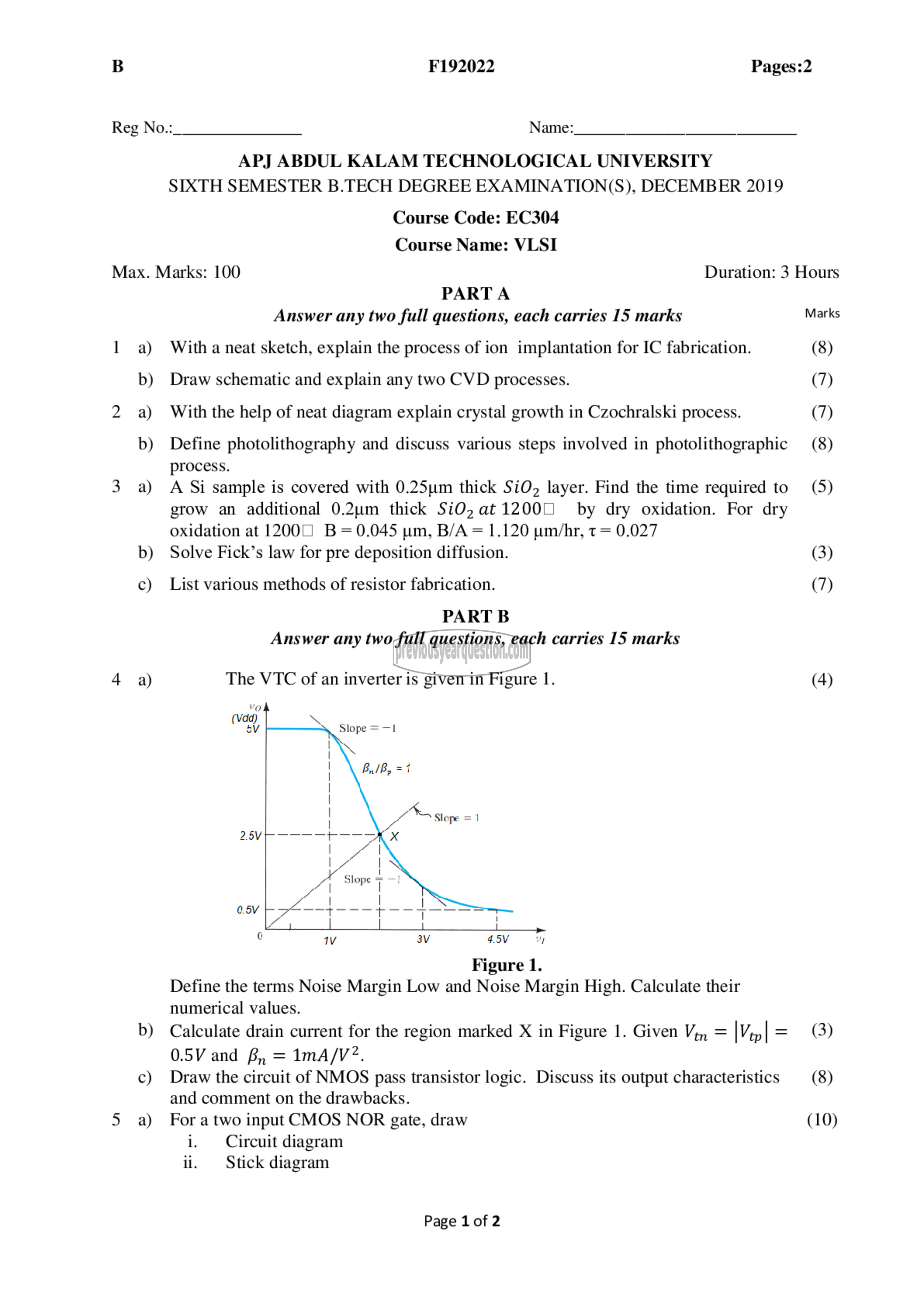
4 a) The VTC of an inverter is given in Figure 1. (4)
Se = -॥
١
Slope >1
2.5V
7 |
ಹೆ
1 |
ہوم ಪಾಲೋ 7 : سے
८ । | | _॥ 1 .
9 10 3۷ 4.5% 1
Figure 1.
Define the terms Noise Margin Low and Noise Margin High. Calculate their
numerical values.
b) Calculate drain current for the region marked X in Figure 1. Given ಗೈ = [४५ | = (3)
0.57 and ہم = 1mA/V?.
c) Draw the circuit of NMOS pass transistor logic. Discuss its output characteristics (8)
and comment on the drawbacks.
5 லி Fora two input CMOS NOR gate, draw (10)
i. Circuit diagram
ii. Stick diagram
Page 1 of 2
