APJ ABDUL KALAM TECHNOLOGICAL UNIVERSITY Previous Years Question Paper & Answer
Semester : SEMESTER 6
Subject : VLSI
Year : 2019
Term : DECEMBER
Scheme : 2015 Full Time
Course Code : EC 304
Page:2
b)
a)
b)
a)
b)
a)
b)
a)
b)
F192022 Pages:2
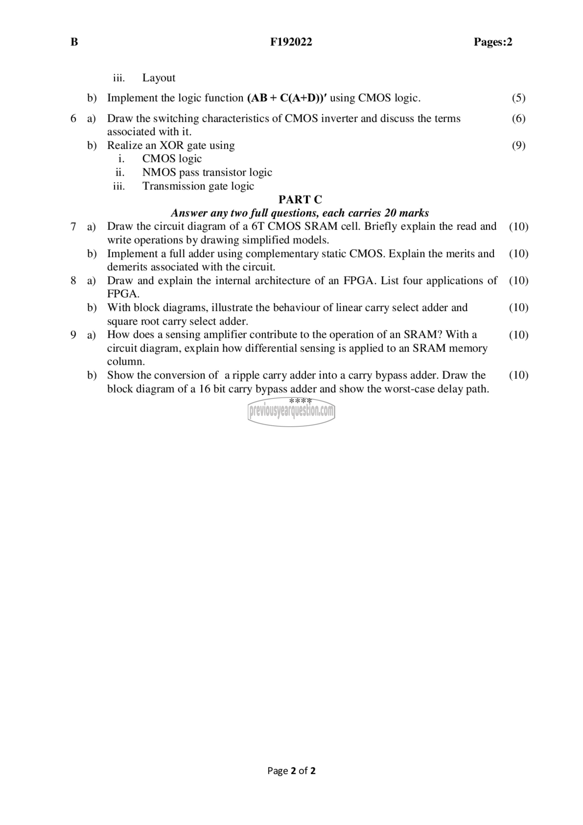
iii. Layout
Implement the logic function (AB + C(A+D))’ using CMOS logic.
Draw the switching characteristics of CMOS inverter and discuss the terms
associated with it.
Realize an XOR gate using
i. CMOS logic
ii. NMOS pass transistor logic
iii. | Transmission gate logic
PART ட
Answer any two full questions, each carries 20 marks
Draw the circuit diagram of a 6T CMOS SRAM cell. Briefly explain the read and
write operations by drawing simplified models.
Implement a full adder using complementary static CMOS. Explain the merits and
demerits associated with the circuit.
Draw and explain the internal architecture of an FPGA. List four applications of
FPGA.
With block diagrams, illustrate the behaviour of linear carry select adder and
square root carry select adder.
How does a sensing amplifier contribute to the operation of an SRAM? With a
circuit diagram, explain how differential sensing is applied to an SRAM memory
column.
Show the conversion of a ripple carry adder into a carry bypass adder. Draw the
block diagram of a 16 bit carry bypass adder and show the worst-case delay path.
Page 2 of 2
(5)
(6)
(9)
(10)
(10)
(10)
(10)
(10)
(10)
