APJ ABDUL KALAM TECHNOLOGICAL UNIVERSITY Previous Years Question Paper & Answer
University : APJ ABDUL KALAM TECHNOLOGICAL UNIVERSITY
Course : B.Tech
Semester : SEMESTER 6
Subject : VLSI
Year : 2021
Term : JULY
Scheme : 2015 Full Time
Course Code : EC 304
Page:2
PDF Text (Beta):
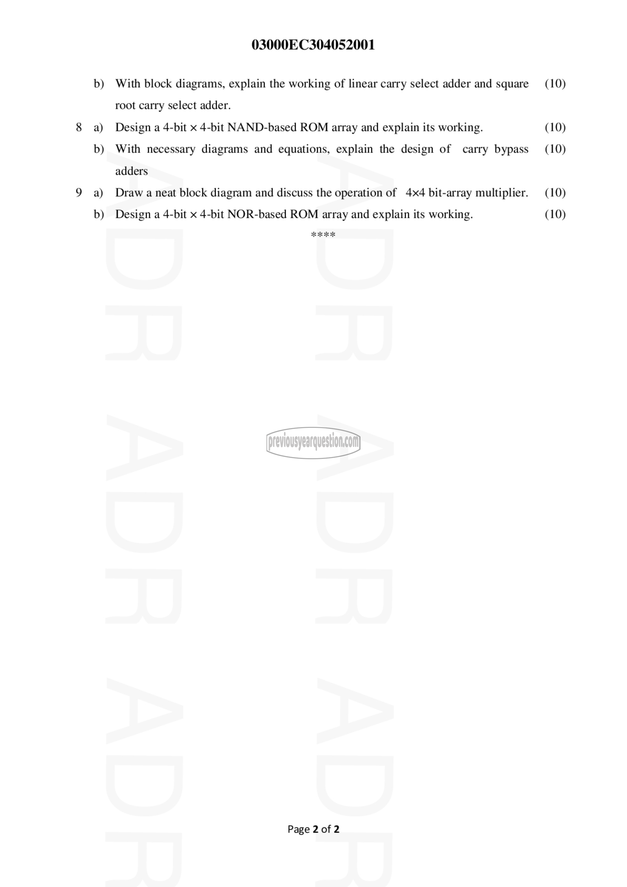
03000EC304052001
With block diagrams, explain the working of linear carry select adder and square
root carry select adder.
Design a 4-bit x 4-bit NAND-based ROM array and explain its working.
With necessary diagrams and equations, explain the design of carry bypass
adders
Draw a neat block diagram and discuss the operation of 4x4 bit-array multiplier.
Design a 4-bit x 4-bit NOR-based ROM array and explain its working.
Page 2 of 2
(10)
(10)
(10)
(10)
(10)
Similar Question Papers
APJ ABDUL KALAM TECHNOLOGICAL UNIVERSITY =>
M.Tech =>
SEMESTER 2 =>
Design of VLSI Systems =>
2017 => APRIL =>
Download
APJ ABDUL KALAM TECHNOLOGICAL UNIVERSITY =>
M.Tech =>
SEMESTER 1 =>
VLSI Technology and Design =>
2021 => APRIL =>
Download
APJ ABDUL KALAM TECHNOLOGICAL UNIVERSITY =>
M.Tech =>
SEMESTER 2 =>
Design of VLSI Systems =>
2016 => MAY =>
Download
APJ ABDUL KALAM TECHNOLOGICAL UNIVERSITY =>
B.Tech =>
SEMESTER 5 =>
VLSI Circuit Design =>
2020 => DECEMBER =>
Download
APJ ABDUL KALAM TECHNOLOGICAL UNIVERSITY =>
B.Tech =>
SEMESTER 6 =>
VLSI =>
2021 => JULY =>
Download
