APJ ABDUL KALAM TECHNOLOGICAL UNIVERSITY Previous Years Question Paper & Answer
Semester : SEMESTER 3
Subject : Switching Theory and Logic Design
Year : 2022
Term : JANUARY
Branch : COMPUTER SCIENCE AND ENGINEERING
Scheme : 2015 Full Time
Course Code : CS 203
Page:2
11
12
13
14
15
16
17
18
19
20
a)
b)
a)
b)
a)
b)
0)
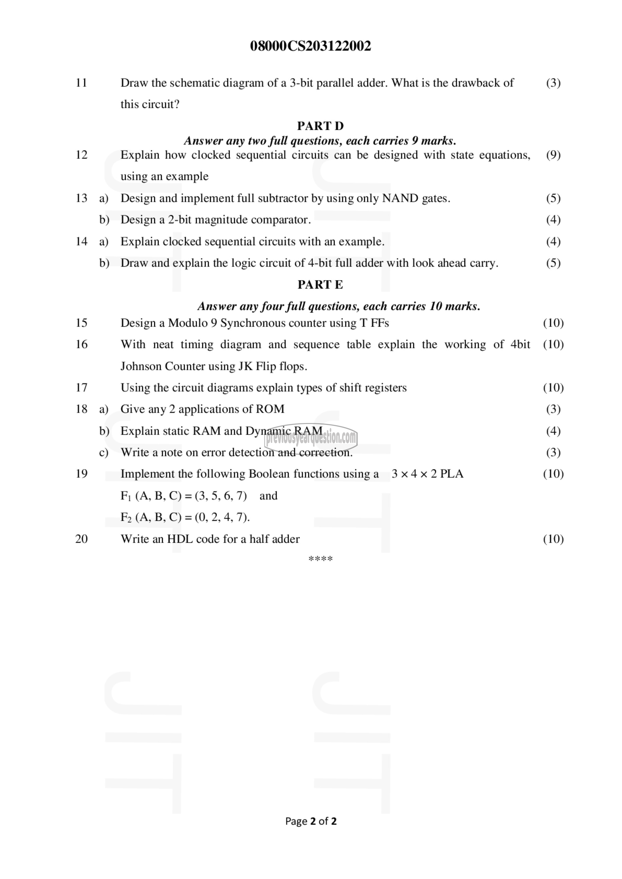
08000CS203122002
Draw the schematic diagram of a 3-bit parallel adder. What is the drawback of
this circuit?
PART 0
Answer any two full questions, each carries 9 marks.
Explain how clocked sequential circuits can be designed with state equations,
using an example
Design and implement full subtractor by using only NAND gates.
Design a 2-bit magnitude comparator.
Explain clocked sequential circuits with an example.
Draw and explain the logic circuit of 4-bit full adder with look ahead carry.
PART E
Answer any four full questions, each carries 10 marks.
Design a Modulo 9 Synchronous counter using T FFs
With neat timing diagram and sequence table explain the working of 4bit
Johnson Counter using JK Flip flops.
Using the circuit diagrams explain types of shift registers
Give any 2 applications of ROM
Explain static RAM and Dynamic RAM
Write a note on error detection and correction.
Implement the following Boolean functions usinga 3x4x2PLA
F; (A, 8, C) = (3, 5,6, 7) 84
1 (A, 8, C) = (0, 2, 4, 7).
Write an HDL code for a half adder
Page 2 of 2
(3)
(9)
(5)
(4)
(4)
(5)
(10)
(10)
(10)
(3)
(4)
(3)
(10)
(10)
