APJ ABDUL KALAM TECHNOLOGICAL UNIVERSITY Previous Years Question Paper & Answer
Semester : SEMESTER 3
Subject : Logic Circuit Design
Year : 2018
Term : APRIL
Scheme : 2015 Full Time
Course Code : EC 207
Page:1
E E3836 Pages: 2
Reg No.: Name:
APJ ABDUL KALAM TECHNOLOGICAL UNIVERSITY
THIRD SEMESTER B.TECH DEGREE EXAMINATION, APRIL 2018
Course Code: EC207
Course Name: LOGIC CIRCUIT DESIGN (EC, AE)
Max. Marks: 100 Duration: 3 Hours
PARTA
Answer any two full questions, each carries 15 marks Marks
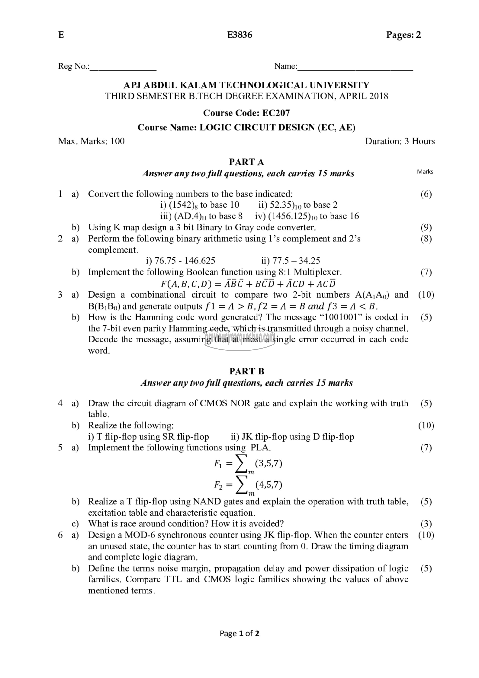
1 a) Convert the following numbers to the base indicated: (6)
i) (1542)8 10 base 10 11) 52.35) to base 2
11) (AD.4)q to base 8 1५) (1456.125)10 to base 16
b) Using K map design a 3 bit Binary to Gray code converter. (9)
2 a) Perform the following binary arithmetic using 1’s complement and 2’s (8)
complement.
i) 76.75 - 146.625 ii) 77.5 — 34.25
b) Implement the following Boolean function using 8:1 Multiplexer. (7)
F(A,B,C,D) = ABC + BCD + ACD + ACD
3 8) Design a combinational circuit to compare two 2-bit numbers ಗಗ ಗಿ) and (10)
B(B;Bo) and generate outputs f1 = 4 > 5, {2 = 4 = 8 0710/3 = 4 > 9.
b) How is the Hamming code word generated? The message “1001001” is coded 111 (5)
the 7-bit even parity Hamming code, which is transmitted through a noisy channel.
Decode the message, assuming that at most a single error occurred in each code
word.
PART B
Answer any two full questions, each carries 15 marks
4 a) Draw the circuit diagram of CMOS NOR gate and explain the working with truth (5)
table.
b) Realize the following: (10)
i) T flip-flop using SR flip-flop ii) JK flip-flop using D flip-flop
5 a) Implement the following functions using PLA. (7)
R=) தேற
سنا
ديم (45,7)
771
b) Realize aT flip-flop using NAND gates and explain the operation with truth table, (5)
excitation table and characteristic equation.
c) What is race around condition? How it is avoided? (3)
6 a) Designa MOD-6 synchronous counter using JK flip-flop. When the counter enters (10)
an unused state, the counter has to start counting from 0. Draw the timing diagram
and complete logic diagram.
b) Define the terms noise margin, propagation delay and power dissipation of logic (5)
families. Compare TTL and CMOS logic families showing the values of above
mentioned terms.
Page 1 of 2
