APJ ABDUL KALAM TECHNOLOGICAL UNIVERSITY Previous Years Question Paper & Answer
Semester : SEMESTER 3
Subject : Solid State Devices
Year : 2017
Term : JULY
Scheme : 2015 Full Time
Course Code : EC 203
Page:2
B3C053S Pages: 3
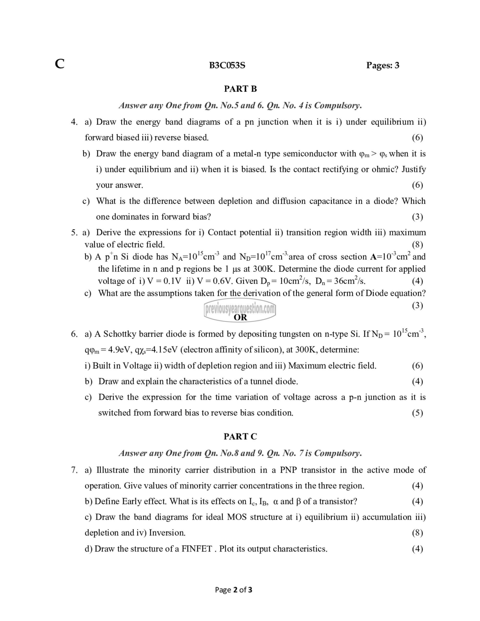
PART B
Answer any One from Qn. No.5 and 6. Qn. No. 4 is Compulsory.
. a) Draw the energy band diagrams of a pn junction when it is i) under equilibrium ii)
forward biased iii) reverse biased. (6)
b) Draw the energy band diagram of a metal-n type semiconductor with وم > ہم when it is
i) under equilibrium and ii) when it is biased. Is the contact rectifying or ohmic? Justify
your answer. (6)
c) What is the difference between depletion and diffusion capacitance in a diode? Which
one dominates in forward bias? (3)
. a) Derive the expressions for i) Contact potential ii) transition region width iii) maximum
value of electric field. (8)
b) A pn Si diode has Na=10'%cm? and Np=10!cm™ area of cross section 45107 ला and
the lifetime in n and م regions be 1 ts at 300K. Determine the diode current for applied
voltage of 1) ४ = 0.1४ 11) ४ = 0.6४. Given 10, = 10017215, تروط 36۸ (4)
c) What are the assumptions taken for the derivation of the general form of Diode equation?
(3)
OR
. a) A Schottky barrier diode is formed by depositing tungsten on n-type Si. If Np = 10௦0”,
99൦ 4.9eV, qys=4.15eV (electron affinity of silicon), at 300K, determine:
i) Built in Voltage ii) width of depletion region and iii) Maximum electric field. (6)
b) Draw and explain the characteristics of a tunnel diode. (4)
c) Derive the expression for the time variation of voltage across a p-n junction as it is
switched from forward bias to reverse bias condition. (5)
PART C
Answer any One from Qn. No.8 and 9. Qn. No. 7 is Compulsory.
. a) Illustrate the minority carrier distribution in a PNP transistor in the active mode of
operation. Give values of minority carrier concentrations in the three region. (4)
0) Define Early effect. What is its effects on 10, Ip, ७ and 3 of a transistor? (4)
c) Draw the band diagrams for ideal MOS structure at i) equilibrium ii) accumulation 111)
depletion and iv) Inversion. (8)
d) Draw the structure of a FINFET . Plot its output characteristics. (4)
Page 2 of 3
