APJ ABDUL KALAM TECHNOLOGICAL UNIVERSITY Previous Years Question Paper & Answer
Semester : SEMESTER 3
Subject : Solid State Devices
Year : 2018
Term : APRIL
Scheme : 2015 Full Time
Course Code : EC 203
Page:1
^ (3801 Pages: 2
Reg No.: Name:
APJ ABDUL KALAM TECHNOLOGICAL UNIVERSITY
THIRD SEMESTER B.TECH DEGREE EXAMINATION, APRIL 2018
Course Code: EC203
Course Name: SOLID STATE DEVICES (EC, AE)
Max. Marks: 100 Duration: 3 Hours
PART A
Answer any two full questions, each carries 15 marks Marks
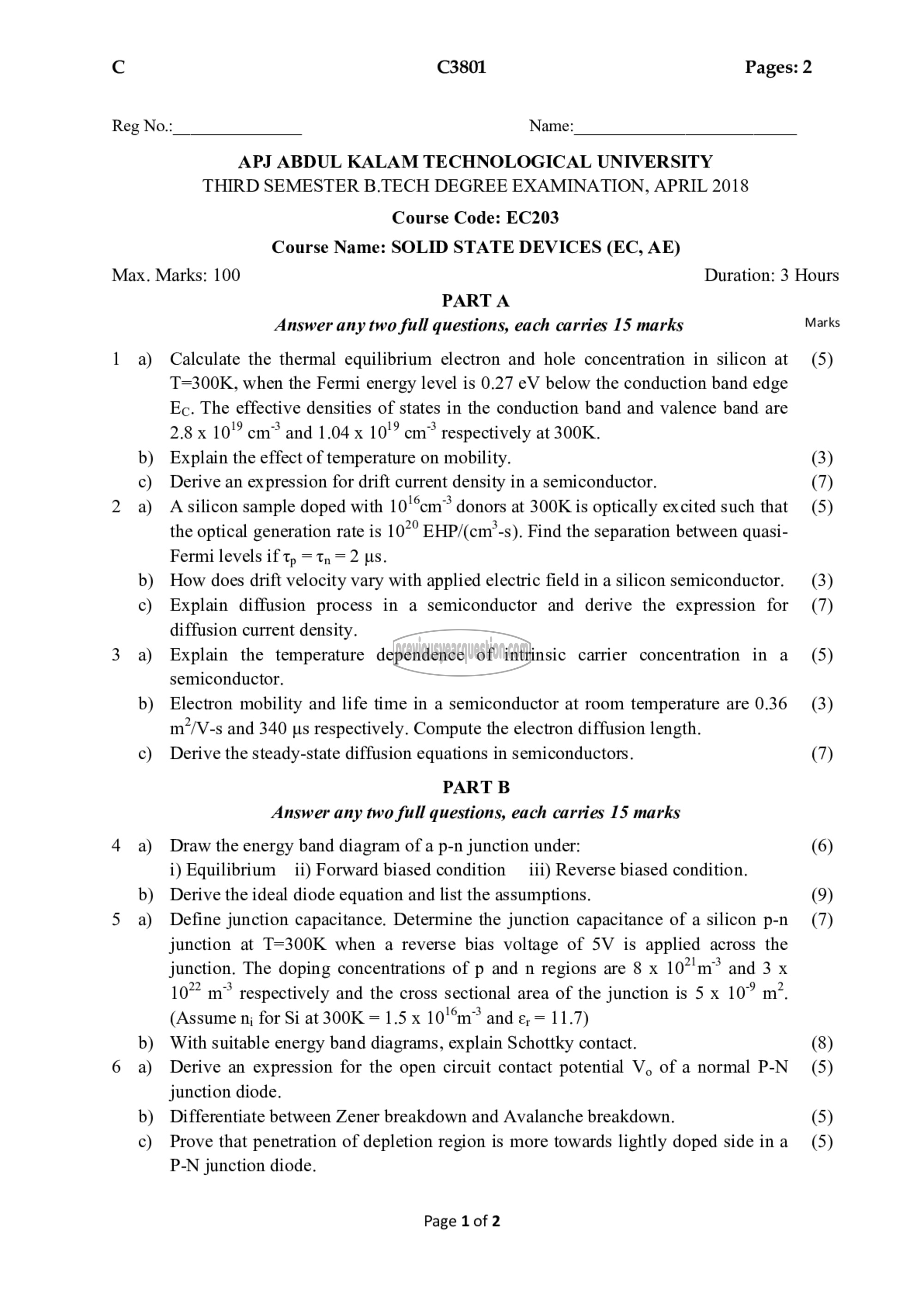
1 8) Calculate the thermal equilibrium electron and hole concentration in silicon at (5)
T=300K, when the Fermi energy level is 0.27 eV below the conduction band edge
Ec. The effective densities of states in the conduction band and valence band are
2.8 x 10⁷ ണ് and 1.04 x 10⁷ അഞ് respectively at 300K.
b) Explain the effect of temperature on mobility. (3)
c) Derive an expression for drift current density in a semiconductor. (7)
2 a) Asilicon sample doped with 1011007 donors at 300K is optically excited such that (5)
the optical generation rate 15 1020 EHP/(cm’-s), Find the separation between quasi-
Fermi levels if फ = ए = 2 us.
b) How does drift velocity vary with applied electric field in a silicon semiconductor. (3)
c) Explain diffusion process in a semiconductor and derive the expression for (7)
diffusion current density.
3 9) Explain the temperature dependence of intrinsic carrier concentration in a (5)
semiconductor.
b) Electron mobility and life time in a semiconductor at room temperature are 0.36 (3)
m’/V-s and 340 us respectively. Compute the electron diffusion length.
c) Derive the steady-state diffusion equations in semiconductors. (7)
PART 8
Answer any two full questions, each carries 15 marks
4 a) Draw the energy band diagram of a p-n junction under: (6)
i) Equilibrium 14) Forward biased condition 111) Reverse biased condition.
b) Derive the ideal diode equation and list the assumptions. (9)
5 a) Define junction capacitance. Determine the junction capacitance of a silicon p-n (7)
junction at T=300K when a reverse bias voltage of 5V is applied across the
junction. The doping concentrations of p and n regions are 8 x 10ന് and 3 x
103 ന് respectively and the cross sectional area of the junction is 5 x 10° خم
(Assume n; for Si at 300K = 1.5 x 10% and £= 11.7)
b) With suitable energy band diagrams, explain Schottky contact. (8)
6 a) Derive an expression for the open circuit contact potential V, of a normal P-N (5)
junction diode.
b) Differentiate between Zener breakdown and Avalanche breakdown. (5)
c) Prove that penetration of depletion region is more towards lightly doped side ina (5)
P-N junction diode.
Page 1 of 2
