APJ ABDUL KALAM TECHNOLOGICAL UNIVERSITY Previous Years Question Paper & Answer
Semester : SEMESTER 3
Subject : Solid State Devices
Year : 2017
Term : DECEMBER
Scheme : 2015 Full Time
Course Code : EC 203
Page:1
Reg No.: Name:
Max. Marks: 100
b)
2 a)
b)
3 a)
b)
4 a)
b)
5 2)
b)
6 a)
b)
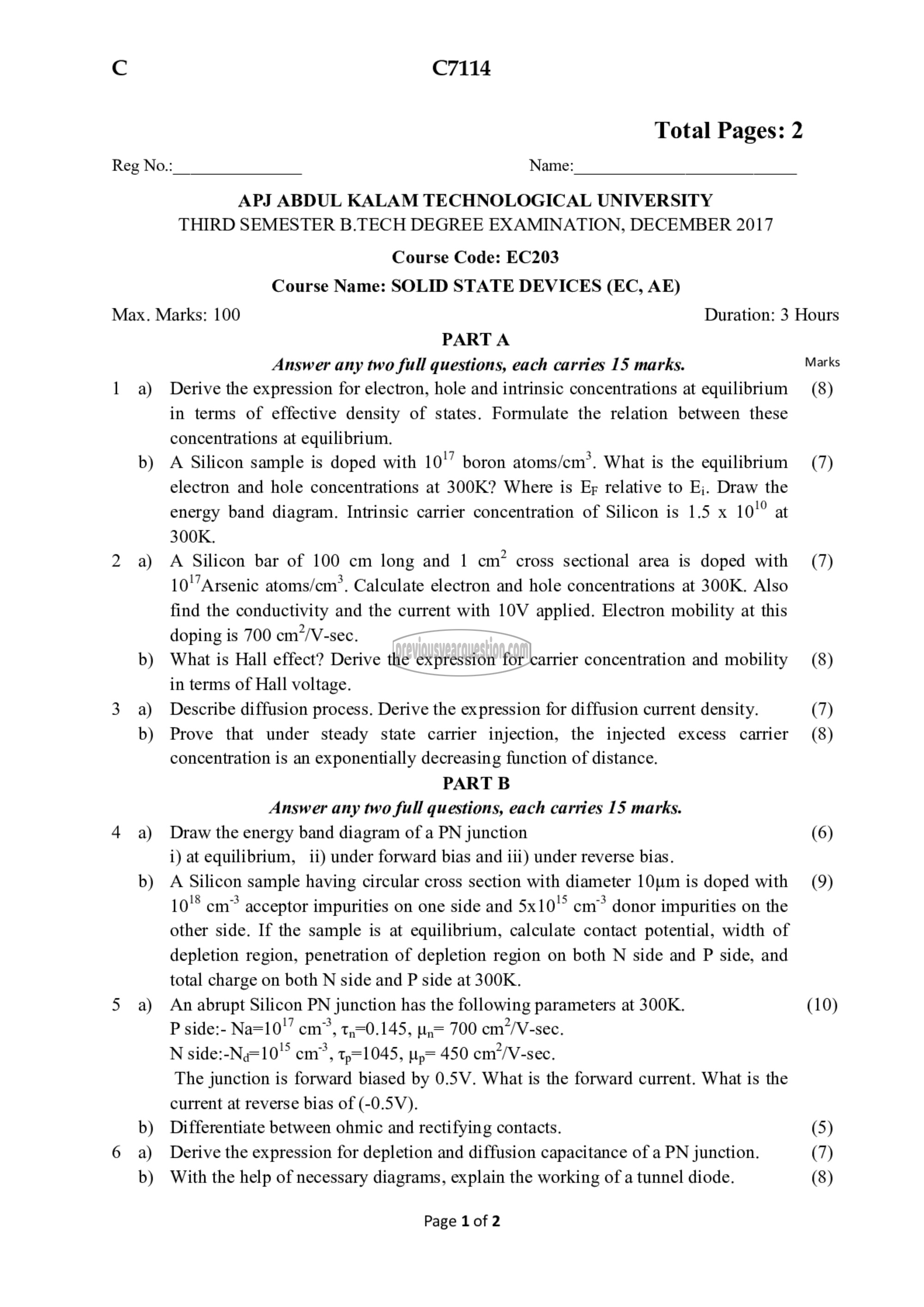
C7114
Total Pages: 2
APJ ABDUL KALAM TECHNOLOGICAL UNIVERSITY
THIRD SEMESTER B.TECH DEGREE EXAMINATION, DECEMBER 2017
Course Code: EC203
Course Name: SOLID STATE DEVICES (EC, AE)
PART A
Answer any two full questions, each carries 15 marks.
Derive the expression for electron, hole and intrinsic concentrations at equilibrium
in terms of effective density of states. Formulate the relation between these
concentrations at equilibrium.
A Silicon sample is doped with 1011 boron atoms/em*. What is the equilibrium
electron and hole concentrations at 300K? Where is நி relative to 1. Draw the
energy band diagram. Intrinsic carrier concentration of Silicon is 1.5 x 10% at
300K.
A Silicon bar of 100 cm long and 1 cm? cross sectional area is doped with
10'’Arsenic atoms/cm’. Calculate electron and hole concentrations at 300K. Also
find the conductivity and the current with 10V applied. Electron mobility at this
doping is 700 ला /५-5९०.
What is Hall effect? Derive the expression for carrier concentration and mobility
in terms of Hall voltage.
Describe diffusion process. Derive the expression for diffusion current density.
Prove that under steady state carrier injection, the injected excess carrier
concentration is an exponentially decreasing function of distance.
PART B
Answer any two full questions, each carries 15 marks.
Draw the energy band diagram of a PN junction
i) at equilibrium, ii) under forward bias and iii) under reverse bias.
A Silicon sample having circular cross section with diameter 10൮൩ is doped with
1015 ഞ് acceptor impurities on one side and 55107 ണ് donor impurities on the
other side. If the sample is at equilibrium, calculate contact potential, width of
depletion region, penetration of depletion region on both N side and P side, and
total charge on both N side and P side at 300K.
An abrupt Silicon PN junction has the following parameters at 300K.
P side:- Na=10!” ഞ്, 1,=0.145, ம” 700 cm?/V-sec.
N side:-N,=10" cm”, T=1045, பூ- 0 cm?/V-sec.
The junction is forward biased by 0.5V. What is the forward current. What is the
current at reverse bias of (-0.5V).
Differentiate between ohmic and rectifying contacts.
Derive the expression for depletion and diffusion capacitance of a PN junction.
With the help of necessary diagrams, explain the working of a tunnel diode.
Page 1 of 2
Duration: 3 Hours
Marks
(8)
(7)
(7)
(8)
(7)
(8)
(6)
(9)
(10)
(5)
(7)
(8)
