APJ ABDUL KALAM TECHNOLOGICAL UNIVERSITY Previous Years Question Paper & Answer
Semester : SEMESTER 3
Subject : Switching Theory and Logic Design
Year : 2017
Term : JULY
Branch : COMPUTER SCIENCE AND ENGINEERING
Scheme : 2015 Full Time
Course Code : CS 203
Page:2
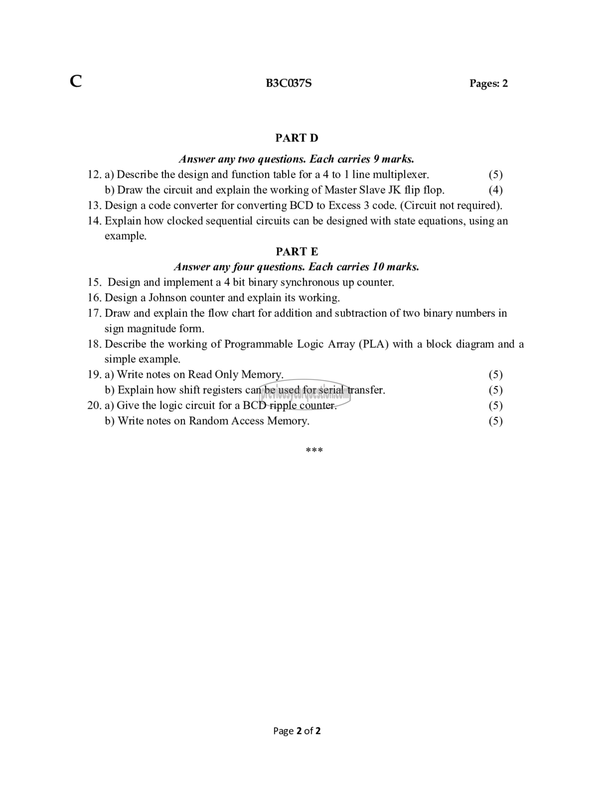
12.
13.
B3C037S Pages: 2
PART D
Answer any two questions. Each carries 9 marks.
a) Describe the design and function table for a 4 to 1 line multiplexer. (5)
b) Draw the circuit and explain the working of Master Slave JK flip flop. (4)
Design a code converter for converting BCD to Excess 3 code. (Circuit not required).
. Explain how clocked sequential circuits can be designed with state equations, using an
example.
PART E
Answer any four questions. Each carries 10 marks.
. Design and implement a 4 bit binary synchronous up counter.
. Design a Johnson counter and explain its working.
. Draw and explain the flow chart for addition and subtraction of two binary numbers in
sign magnitude form.
. Describe the working of Programmable Logic Array (PLA) with a block diagram and a
simple example.
. a) Write notes on Read Only Memory. (5)
b) Explain how shift registers can be used for serial transfer. (5)
. a) Give the logic circuit for a BCD ripple counter. (5)
b) Write notes on Random Access Memory. (5)
கக்க
Page 2 of 2
