APJ ABDUL KALAM TECHNOLOGICAL UNIVERSITY Previous Years Question Paper & Answer
Semester : SEMESTER 6
Subject : VLSI
Year : 2017
Term : DECEMBER
Scheme : 2015 Full Time
Course Code : EC 304
Page:1
Total Pages:
Reg No.: Name:
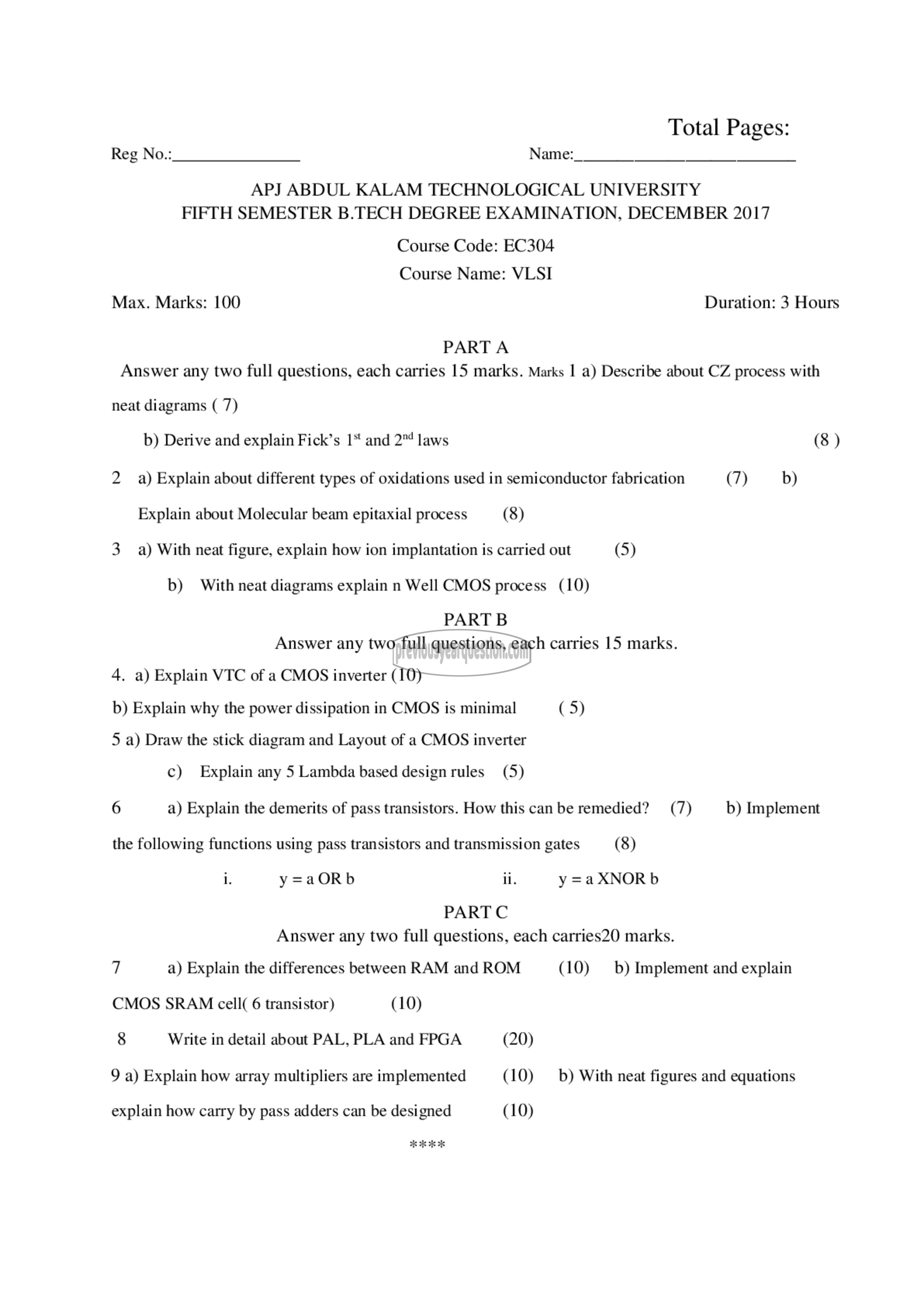
APJ ABDUL KALAM TECHNOLOGICAL UNIVERSITY
FIFTH SEMESTER B.TECH DEGREE EXAMINATION, DECEMBER 2017
Course Code: EC304
Course Name: VLSI
Max. Marks: 100 Duration: 3 Hours
PART A
Answer any two full questions, each carries 15 marks. Marks | a) Describe about CZ process with
neat diagrams ( 7)
b) Derive and explain Fick’s 1“ and 27 laws (8 )
2 9) Explain about different types of oxidations used in semiconductor fabrication (7) b)
Explain about Molecular beam epitaxial process (8)
3 (ہ With neat figure, explain how ion implantation 15 carried out (5)
b) With neat diagrams explain n Well CMOS process (10)
PART 13
Answer any two full questions, each carries 15 marks.
4. a) Explain VTC of a CMOS inverter (10)
b) Explain why the power dissipation in CMOS is minimal (5)
5 a) Draw the stick diagram and Layout of a CMOS inverter
௦) Explain any 5 Lambda based design rules (5)
6 a) Explain the demerits of pass transistors. How this can be remedied? (7) b) Implement
the following functions using pass transistors and transmission gates (8)
i. y=aORb 11. $= 1०१0९२0
२२ ^
Answer any two full questions, each carries20 marks.
7 a) Explain the differences between RAM and ROM (10) 9) Implement and explain
CMOS SRAM cell( 6 transistor) (10)
8 Write in detail about PAL, PLA and FPGA (20)
9 a) Explain how array multipliers are implemented (10) b) With neat figures and equations
explain how carry by pass adders can be designed (10)
