APJ ABDUL KALAM TECHNOLOGICAL UNIVERSITY Previous Years Question Paper & Answer
Semester : SEMESTER 3
Subject : Analog Electronic Circuits
Year : 2018
Term : APRIL
Scheme : 2015 Full Time
Course Code : EE 203
Page:1
Reg No.:
Max. Marks: 100
10
11
12
(a)
(b)
(a)
(b)
(a)
(b)
(a)
(b)
(a)
(b)
(a)
C3807 Pages: 2
Name:
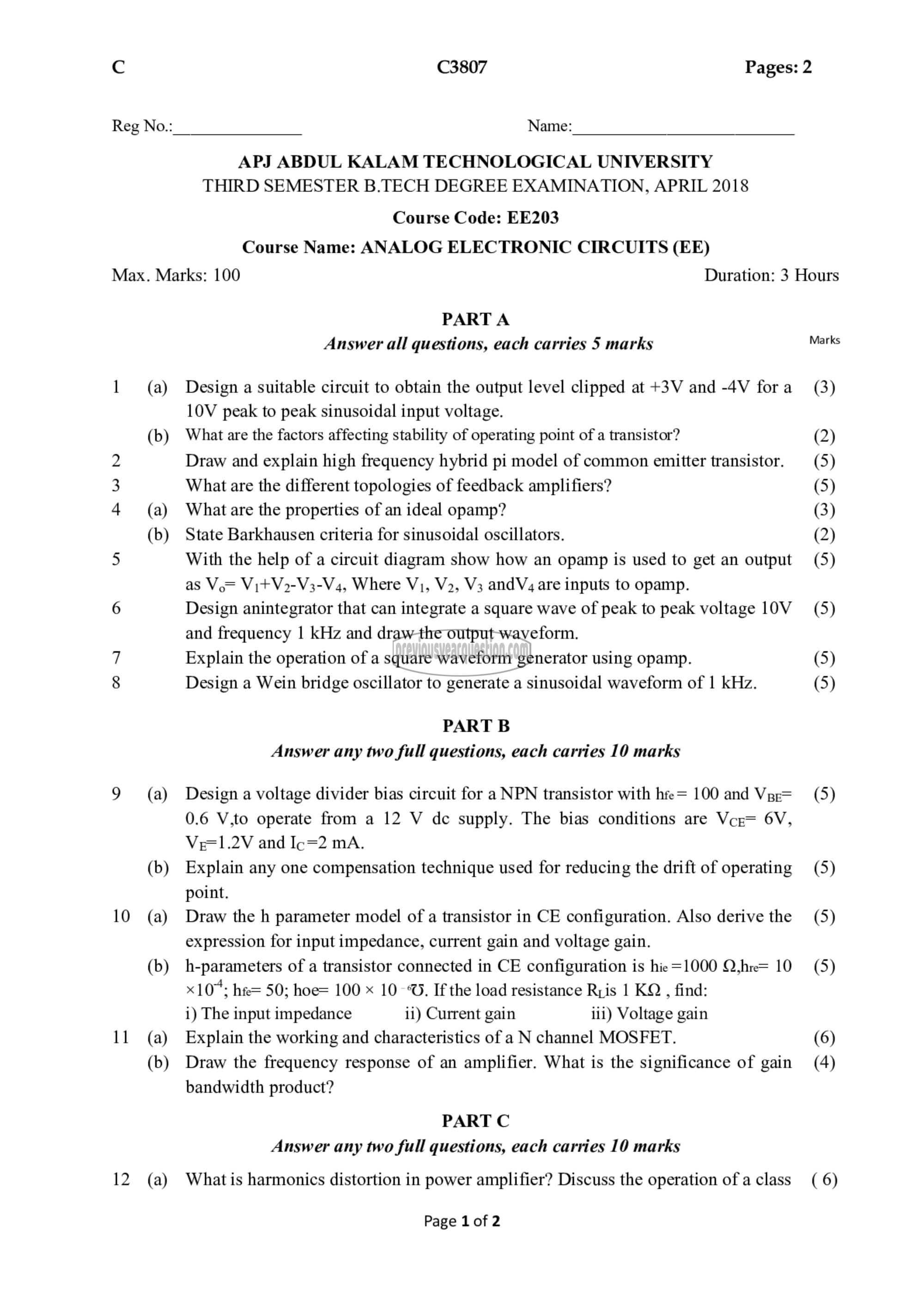
APJ ABDUL KALAM TECHNOLOGICAL UNIVERSITY
THIRD SEMESTER B.TECH DEGREE EXAMINATION, APRIL 2018
Course Code: EE203
Course Name: ANALOG ELECTRONIC CIRCUITS (EE)
PART A
Answer all questions, each carries 5 marks
Design a suitable circuit to obtain the output level clipped at +3V and -4V for a
10V peak to peak sinusoidal input voltage.
What are the factors affecting stability of operating point of a transistor?
Draw and explain high frequency hybrid pi model of common emitter transistor.
What are the different topologies of feedback amplifiers?
What are the properties of an ideal opamp?
State Barkhausen criteria for sinusoidal oscillators.
With the help of a circuit diagram show how an opamp is used to get an output
as ५७०८ Vit V2-V3-V4, Where സഗ. V2, V3 ೩07671, are inputs to opamp.
Design anintegrator that can integrate a square wave of peak to peak voltage 10V
and frequency | kHz and draw the output waveform.
Explain the operation of a square waveform generator using opamp.
Design a Wein bridge oscillator to generate a sinusoidal waveform of 1 kHz.
PART B
Answer any two full questions, each carries 10 marks
Design a voltage divider bias circuit for a NPN transistor with 165 100 and സച
0.6 V,to operate from a 12 V عل supply. The bias conditions are (ए 6V,
Ve=1.2V and Ic=2 mA.
Explain any one compensation technique used for reducing the drift of operating
point.
Draw the h parameter model of a transistor in CE configuration. Also derive the
expression for input impedance, current gain and voltage gain.
h-parameters of a transistor connected in CE configuration 15 hie=1000 Q,hre= 10
105; == 50; hoe= 100 x 10 ൪. If the load resistance [सऽ 1 KQ , find:
i) The input impedance ii) Current gain 111) Voltage gain
Explain the working and characteristics of a N channel MOSFET.
Draw the frequency response of an amplifier. What is the significance of gain
bandwidth product?
PART C
Answer any two full questions, each carries 10 marks
What is harmonics distortion in power amplifier? Discuss the operation of a class
Page 1 of 2
Duration: 3 Hours
Marks
(3)
(2)
(5)
(5)
(3)
(2)
(5)
(5)
(5)
(5)
(5)
(5)
(5)
(5)
(6)
(4)
(6)
