APJ ABDUL KALAM TECHNOLOGICAL UNIVERSITY Previous Years Question Paper & Answer
Semester : SEMESTER 4
Subject : Digital Electronics and Logic Design
Year : 2018
Term : DECEMBER
Scheme : 2015 Full Time
Course Code : EE 204
Page:1
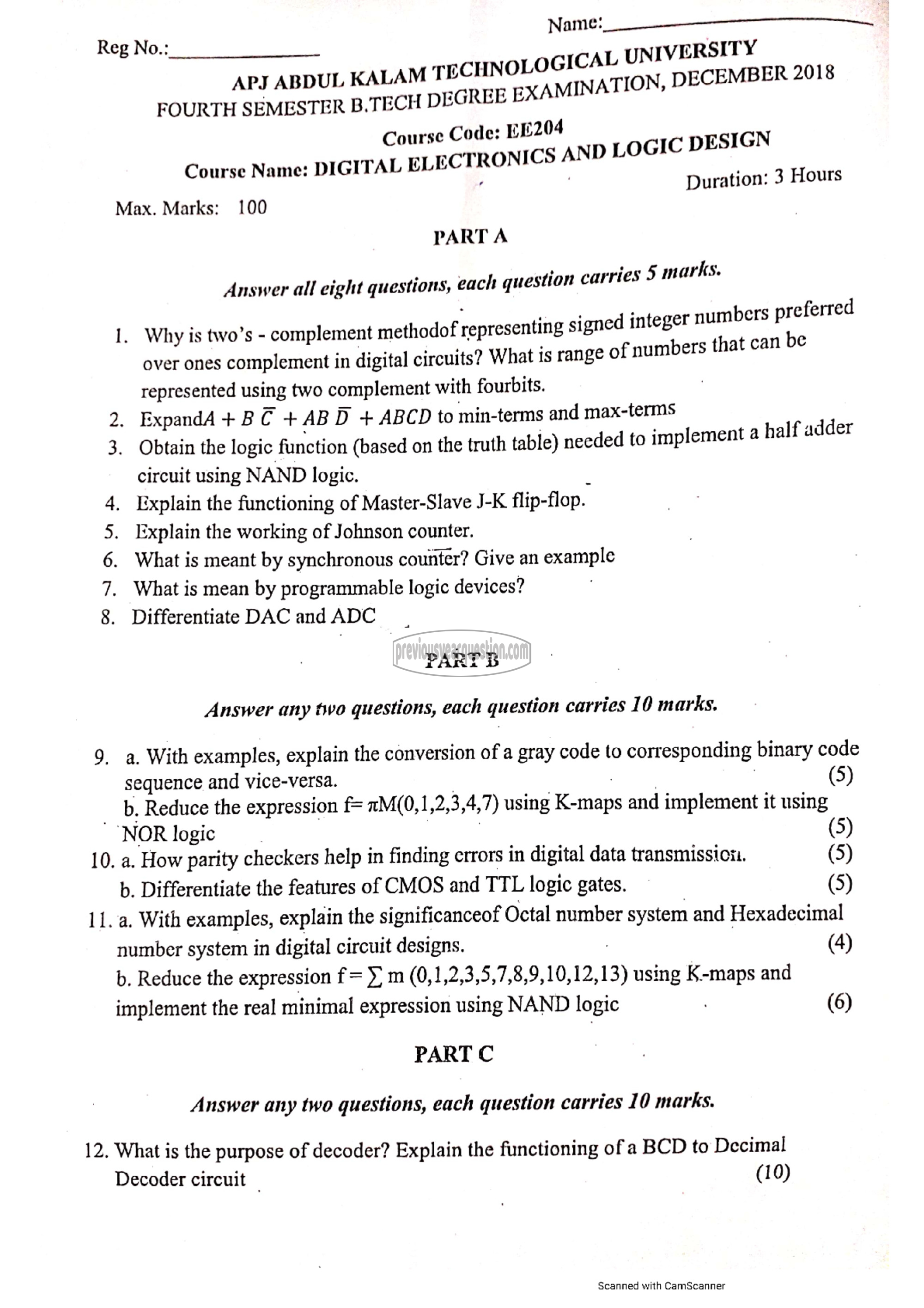
1011८: eS
CHNOLOGICAL UNIVERSITY
Reg No.:
XAMINATION DECEMBER 2018
APJ ABDUL KALAM rE
FOURTH SEMESTER B.TECH DEGREE E
८ 04
ourse Code: 72 LOGIC DESIGN
0 28 T G 5 AND
Cour 5 Name DIG | |
Max. Marks: 100
PART A
each question carries 5 marks.
d integer numbers preferred
f numbers that can be
Answer all eight questions,
Why is two’s - complement methodof representing signe
over ones complement in digital circuits? What 1s range ©
represented using two complement with fourbits
ExpandA + 5 C 48 D + ABCD to min-terms and max-terms
Obtain the logic function (based on the truth table) needed to implement a half adder
circuit using NAND logic
. Explain the functioning of Master-Slave J-K flip-flop
4
5. Explain the working of Johnson counter.
6. What is meant by synchronous counter? Give an example
7
8
I.
. What is mean by programmable logic devices?
. Differentiate DAC andADC =.
PART ॐ
Answer any two questions, each question carries 10 marks.
a. With examples, explain the conversion of a gray code to corresponding binary code
(5)
9,
sequence and vice-versa
b. Reduce the expression f= xM(0,1,2,3,4,7) using K-maps and implement it using
NOR logic (5)
10. a. How parity checkers help in finding crrors in digital data transmission (5)
(5)
b. Differentiate the features of CMOS and TTL logic gates |
11. a. With examples, explain the significanceof Octal number system and Hexadecimal
number system in digital circuit designs (4)
b. Reduce the expression f = 5: m (0,1,2,3,5,7,8,9,10,12,13) using K-maps and
implement the real minimal expression using NAND logic
PART C
(6)
Answer any two questions, each question carries 10 marks.
12, What is the purpose of decoder? Explain the functioning of a BCD to Decimal
(10)
Decoder circuit
Scanned with CamScanner
