APJ ABDUL KALAM TECHNOLOGICAL UNIVERSITY Previous Years Question Paper & Answer
Semester : SEMESTER 3
Subject : ANALOG ELECTRONICS
Year : 2020
Term : DECEMBER
Scheme : 2019 Full Time
Course Code : EET 205
Page:2
13
14
15
16
17
(b)
(a)
(b)
(a)
(b)
(a)
(b)
(a)
(b)
(a)
(b)
0800EET205122003
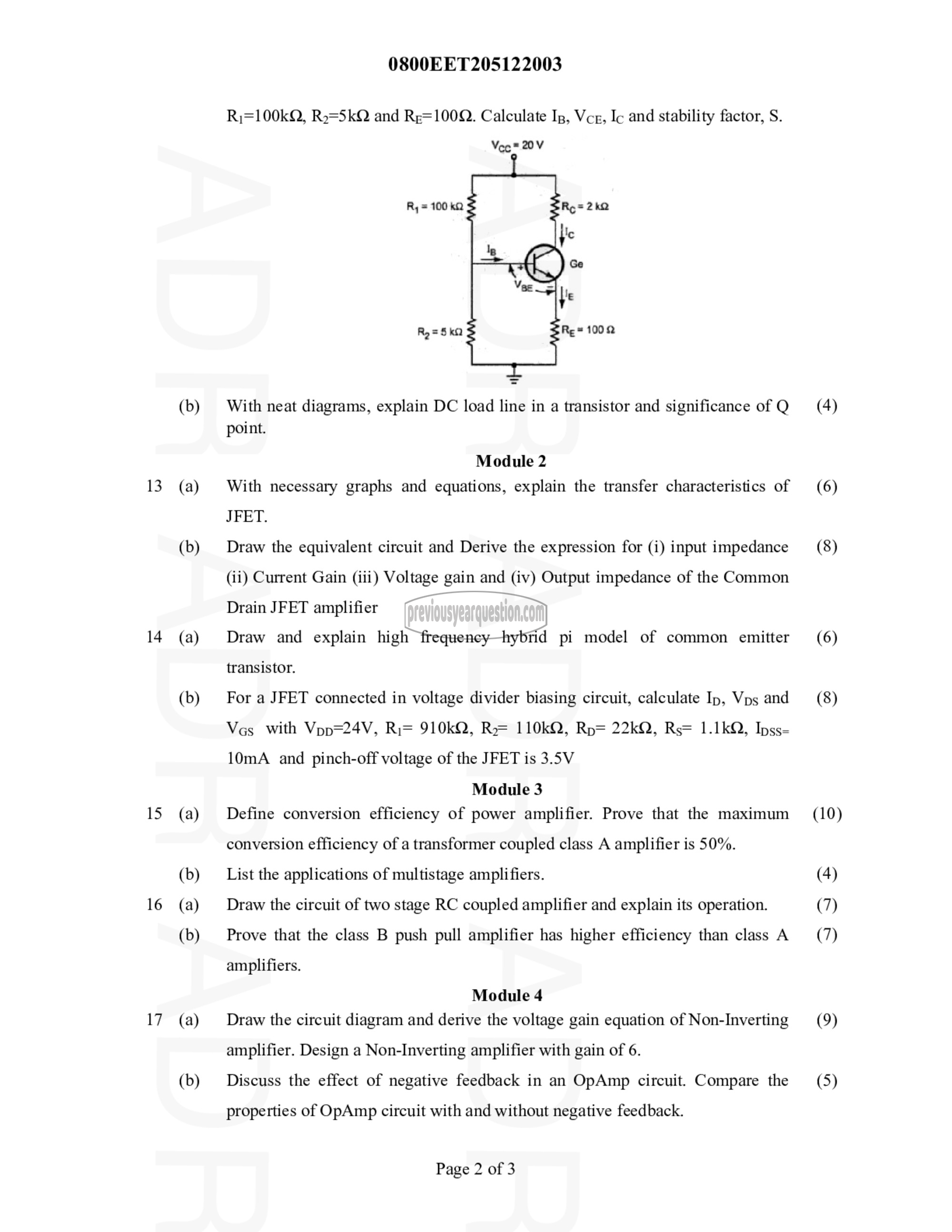
९110013, Ro=5kQ and Re=100Q. Calculate Ip, Vcr, Ic and stability factor, 5.
\८८* 20V
5, = 100 kQ
With neat diagrams, explain DC load line in a transistor and significance of Q
point.
Module 2
With necessary graphs and equations, explain the transfer characteristics of
JFET.
Draw the equivalent circuit and Derive the expression for (i) input impedance
(ii) Current Gain (iii) Voltage gain and (iv) Output impedance of the Common
Drain JFET amplifier
Draw and explain high frequency hybrid pi model of common emitter
transistor.
For a JFET connected in voltage divider biasing circuit, calculate Ip, Vps and
Ves with Vpp=24V, Ri= 910kQ, R= 110kQ, Rp= 22kQ, Rs= 1.1kQ, Ipss-
10mA and pinch-off voltage of the JFET is 3.5V
Module 3
Define conversion efficiency of power amplifier. Prove that the maximum
conversion efficiency of a transformer coupled class A amplifier is 50%.
List the applications of multistage amplifiers.
Draw the circuit of two stage RC coupled amplifier and explain its operation.
Prove that the class B push pull amplifier has higher efficiency than class A
amplifiers.
Module 4
Draw the circuit diagram and derive the voltage gain equation of Non-Inverting
amplifier. Design a Non-Inverting amplifier with gain of 6.
Discuss the effect of negative feedback in an OpAmp circuit. Compare the
properties of OpAmp circuit with and without negative feedback.
Page 2 of 3
(4)
(6)
(8)
(6)
(8)
(10)
(4)
(7)
(7)
(9)
(5)
