APJ ABDUL KALAM TECHNOLOGICAL UNIVERSITY Previous Years Question Paper & Answer
Semester : SEMESTER 3
Subject : Solid State Devices
Year : 2022
Term : JANUARY
Scheme : 2015 Full Time
Course Code : EC 203
Page:2
a)
b)
0)
a)
b)
a)
b)
0)
a)
b)
0)
a)
b)
0)
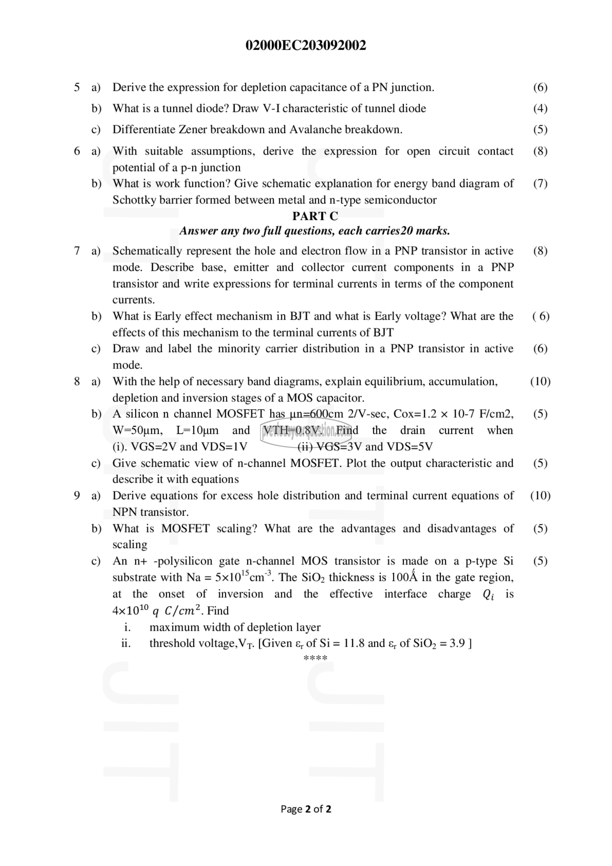
02000EC203092002
Derive the expression for depletion capacitance of a PN junction.
What is a tunnel diode? Draw V-I characteristic of tunnel diode
Differentiate Zener breakdown and Avalanche breakdown.
With suitable assumptions, derive the expression for open circuit contact
potential of a p-n junction
What is work function? Give schematic explanation for energy band diagram of
Schottky barrier formed between metal and n-type semiconductor
PART (^
Answer any two full questions, each carries20 marks.
Schematically represent the hole and electron flow in a PNP transistor in active
mode. Describe base, emitter and collector current components in a PNP
transistor and write expressions for terminal currents in terms of the component
currents.
What is Early effect mechanism in BJT and what is Early voltage? What are the
effects of this mechanism to the terminal currents of BJT
Draw and label the minority carrier distribution in a PNP transistor in active
mode.
With the help of necessary band diagrams, explain equilibrium, accumulation,
depletion and inversion stages of a MOS capacitor.
A silicon ൩ channel MOSFET has pn=600cm 2/V-sec, Cox=1.2 x 10⁻⁷ ۶/۰2,
W=50um, L=l0um and VTH=0.8V. Find the drain current when
(1). VGS=2V and VDS=1V (ii) VGS=3V and VDS=5V
Give schematic view of n-channel MOSFET. Plot the output characteristic and
describe it with equations
Derive equations for excess hole distribution and terminal current equations of
NPN transistor.
What is MOSFET scaling? What are the advantages and disadvantages of
scaling
An n+ -polysilicon gate n-channel MOS transistor is made on a p-type Si
substrate with Na = 5x10'°cm*. The 9102 thickness is 100A in the gate region,
at the onset of inversion and the effective interface charge Q; is
41019 ர C/cm?. Find
i. maximum width of depletion layer
11. _ threshold voltage, V7. [Given ہج of Si= 11.8 and بع of SiO, = 3.9 |
Page 2 of 2
(6)
(4)
(5)
(8)
(7)
(8)
(6)
(6)
(10)
(5)
(5)
(10)
(5)
(5)
