APJ ABDUL KALAM TECHNOLOGICAL UNIVERSITY Previous Years Question Paper & Answer
Semester : SEMESTER 3
Subject : Solid State Devices
Year : 2019
Term : MAY
Scheme : 2015 Full Time
Course Code : EC 203
Page:2
a)
b)
a)
b)
a)
b)
0)
a)
b)
a)
b)
0)
C1115 Pages 2
PART تا
Answer any two full questions, each carries 15 marks.
Draw and explain the VI characteristics of PN junction diode.
Explain the different types of capacitances associated with a p-n junction.
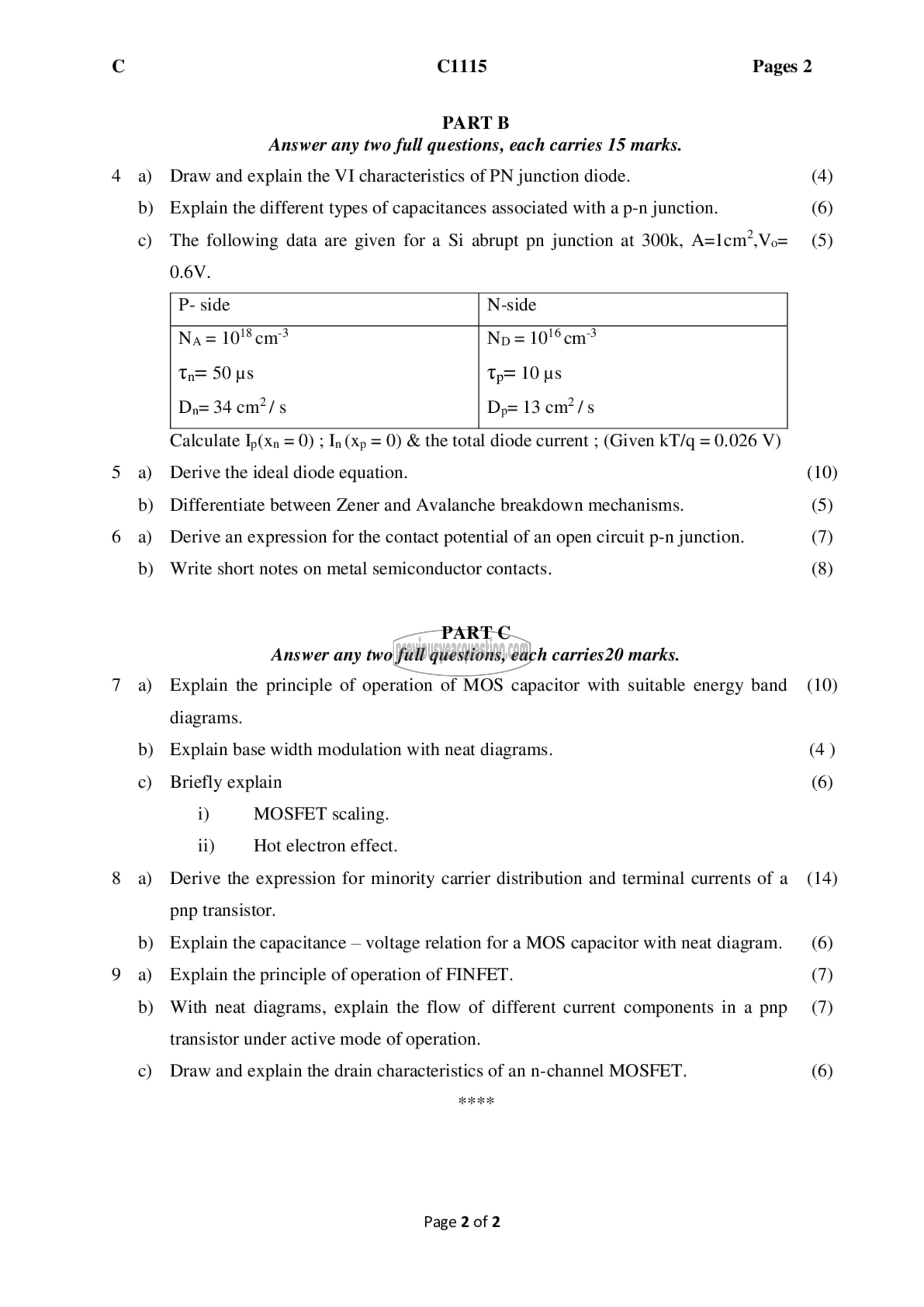
The following data are given for a Si abrupt pn junction at 300k, A=Icm?,Vo=
0.6V.
Na = 1018 cnr? Np = 101900
= 50 us Tp= 10 us
ಎ 34 cm?/s டு 13 cm?/s
Calculate 1900 = 0) ; In(Xp = 0) & the total diode current ; (Given kT/q = 0.026 V)
Derive the ideal diode equation.
Differentiate between Zener and Avalanche breakdown mechanisms.
Derive an expression for the contact potential of an open circuit p-n junction.
Write short notes on metal semiconductor contacts.
PART C
Answer any two full questions, each carries20 marks.
Explain the principle of operation of MOS capacitor with suitable energy band
diagrams.
Explain base width modulation with neat diagrams.
Briefly explain
i) MOSFET scaling.
ii) Hot electron effect.
Derive the expression for minority carrier distribution and terminal currents of a
pnp transistor.
Explain the capacitance — voltage relation for a MOS capacitor with neat diagram.
Explain the principle of operation of FINFET.
With neat diagrams, explain the flow of different current components in a pnp
transistor under active mode of operation.
Draw and explain the drain characteristics of an n-channel MOSFET.
Page 2 of 2
(4)
(6)
(5)
(10)
(5)
(7)
(8)
(10)
(4)
(6)
(14)
(6)
(7)
(7)
(6)
