APJ ABDUL KALAM TECHNOLOGICAL UNIVERSITY Previous Years Question Paper & Answer
Semester : SEMESTER 3
Subject : Logic Circuit Design
Year : 2017
Term : DECEMBER
Scheme : 2015 Full Time
Course Code : EC 207
Page:2
7 ஐ
b)
8 2)
0)
0)
E7253
implemented in PLA.
PART C
Answer any two full questions, each carries 20 marks.
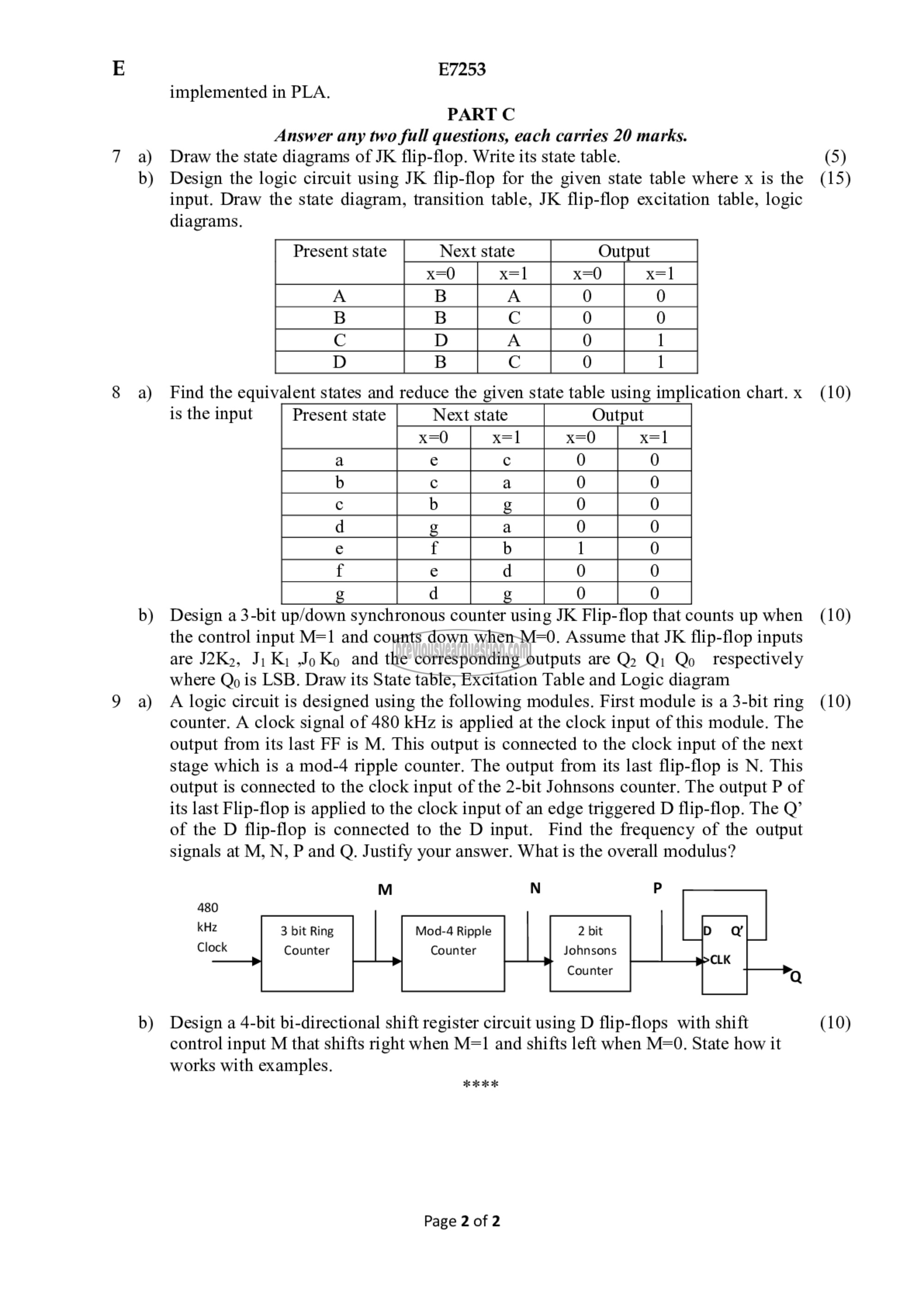
Draw the state diagrams of JK flip-flop. Write its state table.
Design the logic circuit using JK flip-flop for the given state table where x is the
input. Draw the state diagram, transition table, JK flip-flop excitation table, logic
diagrams.
Present state Next state
Design ೩ 3-bit up/down synchronous counter using JK Flip-flop that counts up when
the control input M=1 and counts down when M=0. Assume that JK flip-flop inputs
216 12152, J; Ki Jo Ko and the corresponding outputs are Qo 01 (७ respectively
where Qo is LSB. Draw its State table, Excitation Table and Logic diagram
A logic circuit is designed using the following modules, First module is a 3-bit ring
counter. A clock signal of 480 kHz is applied at the clock input of this module. The
output from its last FF is M. This output is connected to the clock input of the next
stage which is a mod-4 ripple counter. The output from its last flip-flop is N. This
output is connected to the clock input of the 2-bit Johnsons counter. The output P of
its last Flip-flop is applied to the clock input of an edge triggered D flip-flop. The Q’
of the D flip-flop is connected to the D input. Find the frequency of the output
signals at M, N, P and Q. Justify your answer. What is the overall modulus?
M N ۲
480
kHz 3 bit Ring Mod-4 Ripple 2 bit
Clock Counter Counter Johnsons
Counter
Design a 4-bit bi-directional shift register circuit using D flip-flops with shift
control input M that shifts right when M=1 and shifts left when M=0. State how it
works with examples.
ಸೇ मैप اد عد
Page 2 of 2
(5)
(15)
(10)
(10)
(10)
