APJ ABDUL KALAM TECHNOLOGICAL UNIVERSITY Previous Years Question Paper & Answer
Semester : SEMESTER 3
Subject : Solid State Devices
Year : 2020
Term : DECEMBER
Scheme : 2015 Full Time
Course Code : EC 203
Page:2
b)
b)
a)
0)
a)
0)
02000EC203092001
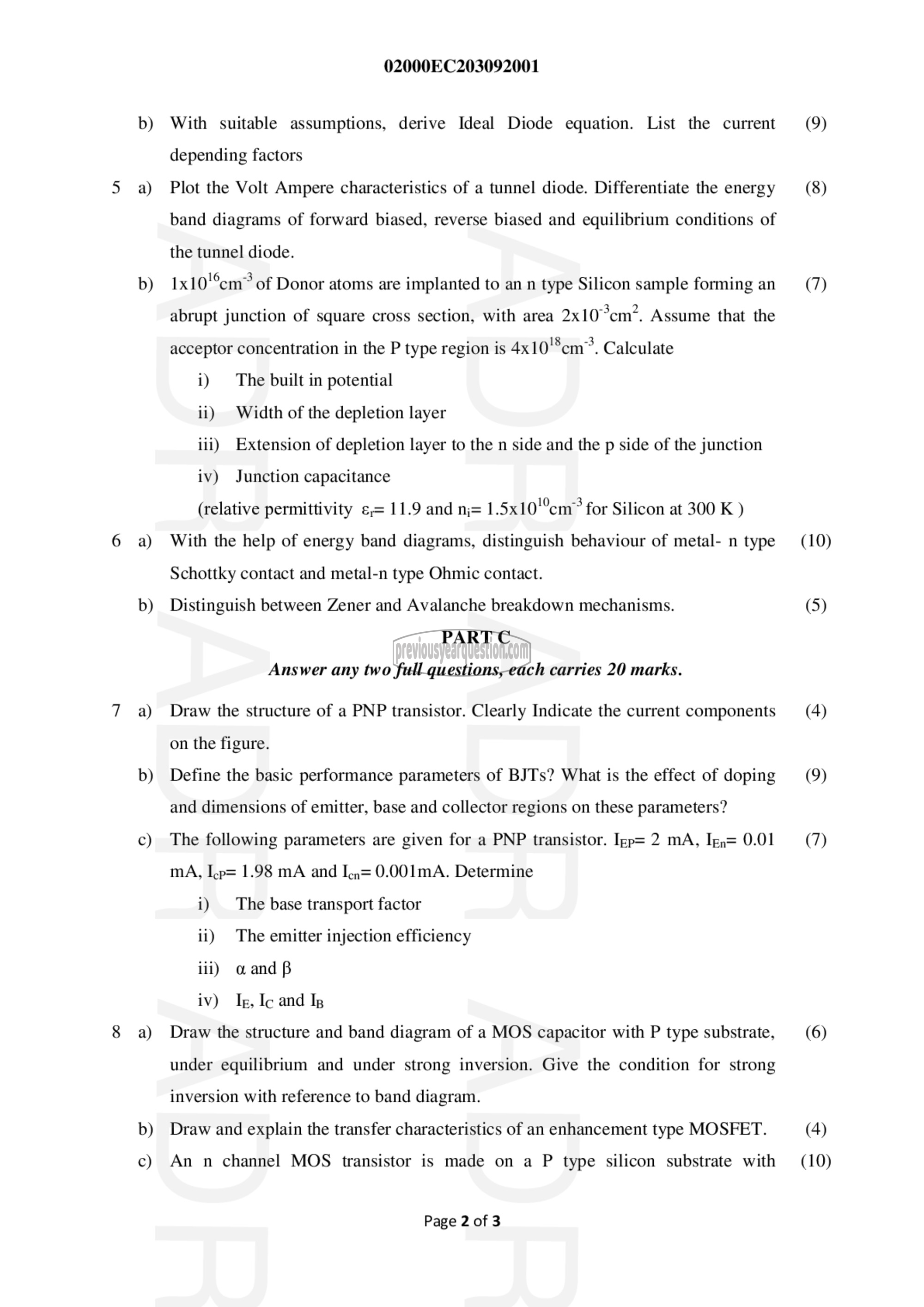
With suitable assumptions, derive Ideal Diode equation. List the current
depending factors
Plot the Volt Ampere characteristics of a tunnel diode. Differentiate the energy
band diagrams of forward biased, reverse biased and equilibrium conditions of
the tunnel diode.
1x10'%cm” of Donor atoms are implanted to an n type Silicon sample forming an
abrupt junction of square cross section, with area 210013, Assume that the
acceptor concentration in the P type region is 4510 ला, Calculate
1) The built in potential
ii) Width of the depletion layer
iii) Extension of depletion layer to the n side and the p side of the junction
iv) Junction capacitance
(relative permittivity ടെ 11.9 and nj= 1.5x10'°cm® for Silicon at 300 K )
With the help of energy band diagrams, distinguish behaviour of metal- n type
Schottky contact and metal-n type Ohmic contact.
Distinguish between Zener and Avalanche breakdown mechanisms.
PART C
Answer any two full questions, each carries 20 marks.
Draw the structure of a PNP transistor. Clearly Indicate the current components
on the figure.
Define the basic performance parameters of BJTs? What is the effect of doping
and dimensions of emitter, base and collector regions on these parameters?
The following parameters are given for a PNP transistor. Igp= 2 mA, [ந 0.01
mA, ಓದ 1.98 mA and 1.15 0.00181۸. Determine
i) The base transport factor
ii) The emitter injection efficiency
iii) ൨൧൧0
iv) 18, Ic and 18
Draw the structure and band diagram of a MOS capacitor with P type substrate,
under equilibrium and under strong inversion. Give the condition for strong
inversion with reference to band diagram.
Draw and explain the transfer characteristics of an enhancement type MOSFET.
An n channel MOS transistor is made on a P type silicon substrate with
Page 2 of 3
(9)
(8)
(7)
(10)
(5)
(4)
(9)
(7)
(6)
(4)
(10)
