APJ ABDUL KALAM TECHNOLOGICAL UNIVERSITY Previous Years Question Paper & Answer
Semester : SEMESTER 5
Subject : Power ElectronEE305ics
Year : 2017
Term : DECEMBER
Scheme : 2015 Full Time
Course Code : EE 305
Page:1
(0 C7056
Total Pages: 2
Reg No.: Name:
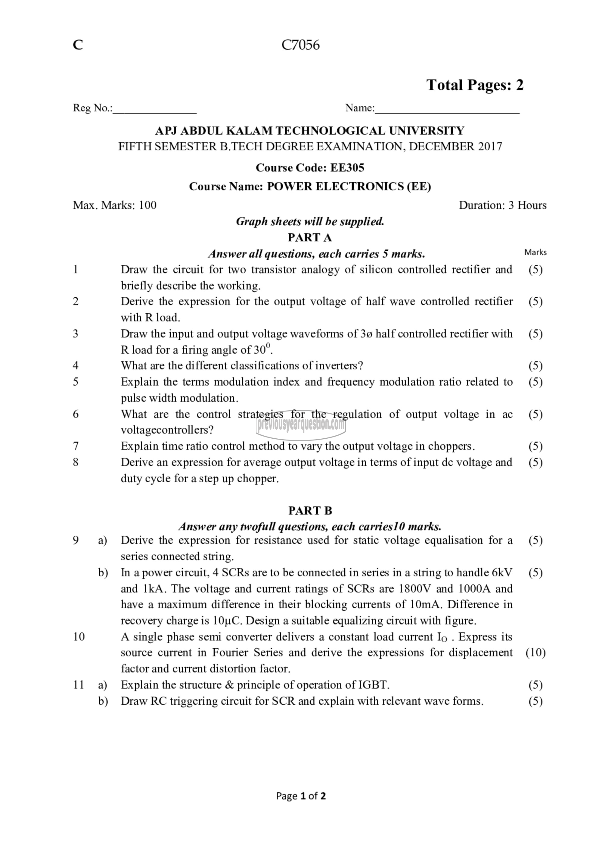
APJ ABDUL KALAM TECHNOLOGICAL UNIVERSITY
FIFTH SEMESTER B.TECH DEGREE EXAMINATION, DECEMBER 2017
Course Code: EE305
Course Name: POWER ELECTRONICS (EE)
Marks
(5)
(5)
Max. Marks: 100 Duration: 3 Hours
Graph sheets will be supplied.
PART A
Answer all questions, each carries 5 marks.
1 Draw the circuit for two transistor analogy of silicon controlled rectifier and
briefly describe the working.
2 Derive the expression for the output voltage of half wave controlled rectifier
with R load.
3 Draw the input and output voltage waveforms of 39 half controlled rectifier with
R load for a firing angle of 30°.
What are the different classifications of inverters?
5 Explain the terms modulation index and frequency modulation ratio related to
pulse width modulation.
6 What are the control strategies for the regulation of output voltage in ac
voltagecontrollers?
7 Explain time ratio control method to vary the output voltage in choppers.
8 Derive an expression for average output voltage in terms of input de voltage and
duty cycle for a step up chopper.
PART B
Answer any twofull questions, each carries10 marks.
9 ಬ Derive the expression for resistance used for static voltage equalisation for a
series connected string.
b) Ina power circuit, 4 SCRs are to be connected in series in a string to handle 6kV
and 1kA. The voltage and current ratings of SCRs are 1800V and 1000A and
have a maximum difference in their blocking currents of 10mA. Difference in
recovery charge is 100. Design ೩ suitable equalizing circuit with figure.
10 A single phase semi converter delivers a constant load current Io . Express its
source current in Fourier Series and derive the expressions for displacement
factor and current distortion factor.
11 ஐ Explain the structure & principle of operation of IGBT.
b) Draw RC triggering circuit for SCR and explain with relevant wave forms.
Page 1 of 2
(5)
(5)
(5)
(5)
(5)
(5)
(5)
(5)
(10)
(5)
(5)
