APJ ABDUL KALAM TECHNOLOGICAL UNIVERSITY Previous Years Question Paper & Answer
Semester : SEMESTER 3
Subject : Electronics Devices & Circuits
Year : 2018
Term : APRIL
Branch : COMPUTER SCIENCE AND ENGINEERING
Scheme : 2015 Full Time
Course Code : CS 207
Page:2
12
13
14
15
16
17
18
19
20
a)
b)
E3842 Pages: 2
PART D
Answer any two full questions, each carries 9 marks
Draw the circuit of an RC coupled amplifier and explain the function of each
element. Sketch the frequency response and write the reasons for gain reduction in
both ends.
Draw the circuit of an astable multivibrator using transistors and explain its
working with a sketch of the waveforms at the collector and base terminals of both
the transistors.
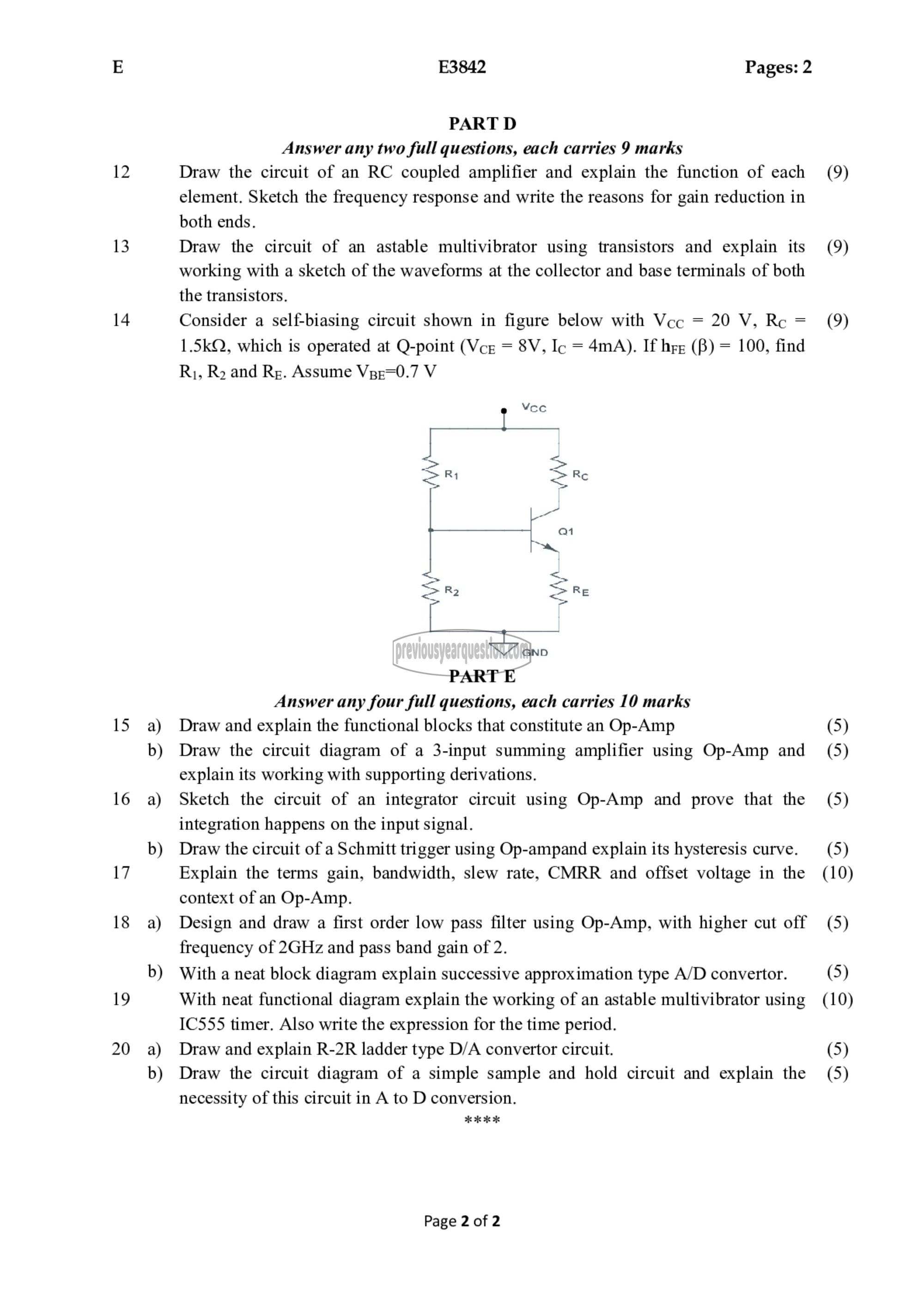
Consider a self-biasing circuit shown in figure below with Vcc = 20 V, Rc =
1.5kQ, which is operated at Q-point (४८६ = 8V, Ic = 4൩൧). If ععط (0) = 100, find
R;, २2 and Rg. Assume Vpr=0.7 7
PART E
Answer any four full questions, each carries 10 marks
Draw and explain the functional blocks that constitute an Op-Amp
Draw the circuit diagram of a 3-input summing amplifier using Op-Amp and
explain its working with supporting derivations.
Sketch the circuit of an integrator circuit using Op-Amp and prove that the
integration happens on the input signal.
Draw the circuit of a Schmitt trigger using Op-ampand explain its hysteresis curve.
Explain the terms gain, bandwidth, slew rate, CMRR and offset voltage in the
context of an Op-Amp.
Design and draw a first order low pass filter using Op-Amp, with higher cut off
frequency of 2GHz and pass band gain of 2.
With a neat block diagram explain successive approximation type A/D convertor.
With neat functional diagram explain the working of an astable multivibrator using
10555 timer. Also write the expression for the time period.
Draw and explain R-2R ladder type D/A convertor circuit.
Draw the circuit diagram of a simple sample and hold circuit and explain the
necessity of this circuit in A to D conversion.
36 عاد ಶೇತೇ
Page 2 of 2
(9)
(9)
(9)
(5)
(5)
(5)
(5)
(10)
(5)
(5)
(10)
(5)
(5)
