APJ ABDUL KALAM TECHNOLOGICAL UNIVERSITY Previous Years Question Paper & Answer
Semester : SEMESTER 3
Subject : Solid State Devices
Year : 2020
Term : SEPTEMBER
Scheme : 2015 Full Time
Course Code : EC 203
Page:1
00000EC203121902
Pages: 2
Reg No.: Name:
Max. Marks: 100
b)
0)
0)
0)
0)
0)
0)
APJ ABDUL KALAM TECHNOLOGICAL UNIVERSITY
Third semester B.Tech examinations (S) September 2020
Course Code: EC203
Course Name: SOLID STATE DEVICES (EC,AE)
PARTA
Answer any two full questions, each carries 15 marks.
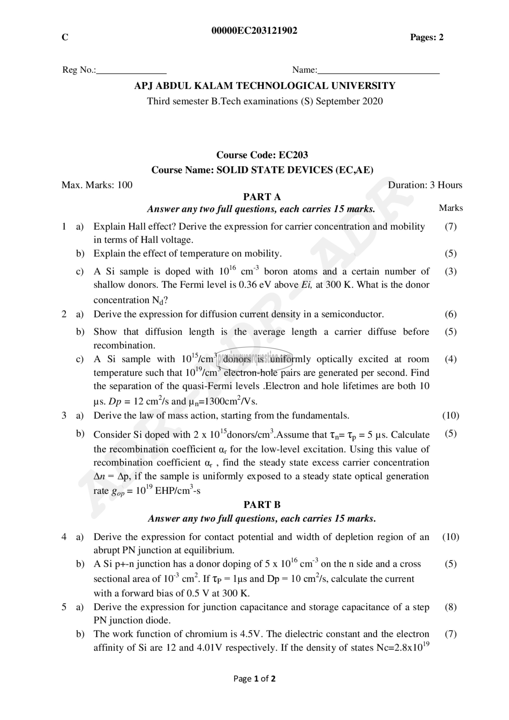
Explain Hall effect? Derive the expression for carrier concentration and mobility
in terms of Hall voltage.
Explain the effect of temperature on mobility.
A Si sample is doped with 10' ഞ് boron atoms and a certain number of
shallow donors. The Fermi level is 0.36 eV above Ei, at 300 K. What is the donor
concentration Ng?
Derive the expression for diffusion current density in a semiconductor.
Show that diffusion length is the average length a carrier diffuse before
recombination.
A Si sample with 10'°/em* donors. is uniformly optically excited at room
temperature such that 10'°/em? electron-hole pairs are generated per second. Find
the separation of the quasi-Fermi levels .Electron and hole lifetimes are both 10
us. Dp = 12 cm’/s and 5130001275.
Derive the law of mass action, starting from the fundamentals.
Consider Si doped with 2 x 10'°donors/em*.Assume that ಟ್ Tp = 5 us. Calculate
the recombination coefficient ہہ for the low-level excitation. Using this value of
recombination coefficient ہہ + find the steady state excess carrier concentration
An = Ap, if the sample is uniformly exposed to a steady state optical generation
rate رمع = 107 EHP/cm*-s
PART छ
Answer any two full questions, each carries 15 marks.
Derive the expression for contact potential and width of depletion region of an
abrupt PN junction at equilibrium.
A Si p+-n junction has a donor doping of 5 x 10 ബ്” on the n side and a cross
sectional area of 10° cm”. If Tp = lps and Dp = 10 cm’/s, calculate the current
with a forward bias of 0.5 V at 300 K.
Derive the expression for junction capacitance and storage capacitance of a step
PN junction diode.
The work function of chromium is 4.5V. The dielectric constant and the electron
affinity of Si are 12 and 4.01۷ respectively. If the density of states Nc=2.8x10"
Page 1 of 2
Duration: 3 Hours
Marks
(7)
(5)
(3)
(6)
(5)
(4)
(10)
(5)
(10)
(5)
(8)
(7)
