APJ ABDUL KALAM TECHNOLOGICAL UNIVERSITY Previous Years Question Paper & Answer
Semester : SEMESTER 1
Subject : Power Converter Circuits
Year : 2017
Term : DECEMBER
Branch : POWER CONTROL AND DRIVES
Scheme : 2015 Full Time
Course Code : 01 EE 6501
Page:1
No. of Pages: 2
APJ ABDUL KALAM TECHNOLOGICAL UNIVERSITY
FIRST SEMESTER M.TECH DEGREE EXAMINATION, DECEMBER 2017
Branch: Electrical & Electronics Engineering
Stream: Power Control and Drives
OIEE6SO1: POWER CONVERTER CIRCUITS
Answer any twofull questions from each part
Limit answers to the required points.
Max. Marks: 60 Duration: 3 hours
PART -A
1.8) Explain the effect of source inductance ina 30 full bridge diode rectificr having highly
inductive load. Draw the relevant waveforms (6) b) Explain line current distortion.
(3)
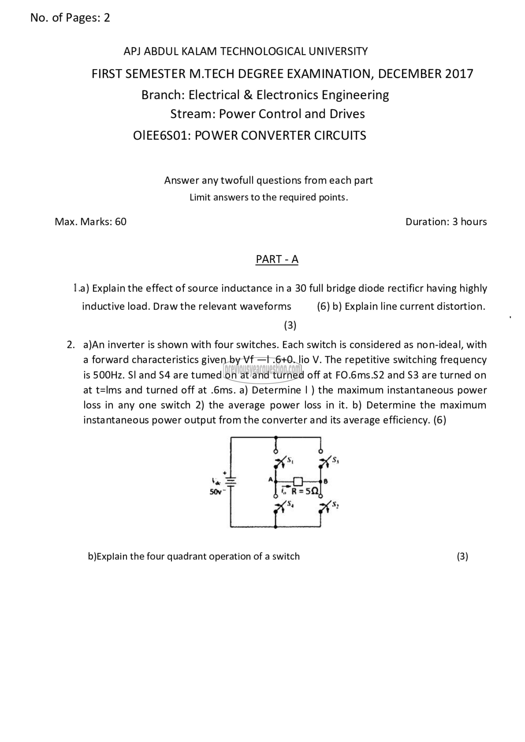
2. a)An inverter is shown with four switches. Each switch is considered as non-ideal, with
a forward characteristics given by Vf --| .6+0. lio V. The repetitive switching frequency
15 500112. 51 and 54 are tumed on at and turned off at FO.6ms.S2 and 53 are turned on
at t=Ims and turned off at .6ms. a) Determine | ) the maximum instantaneous power
loss in any one switch 2) the average power loss in it. b) Determine the maximum
instantaneous power output from the converter and its average efficiency. (6)
b)Explain the four quadrant operation of a switch (3)
