APJ ABDUL KALAM TECHNOLOGICAL UNIVERSITY Previous Years Question Paper & Answer
Semester : SEMESTER 3
Subject : Solid State Devices
Year : 2018
Term : DECEMBER
Scheme : 2015 Full Time
Course Code : EC 203
Page:2
© R3919 Pages: 2
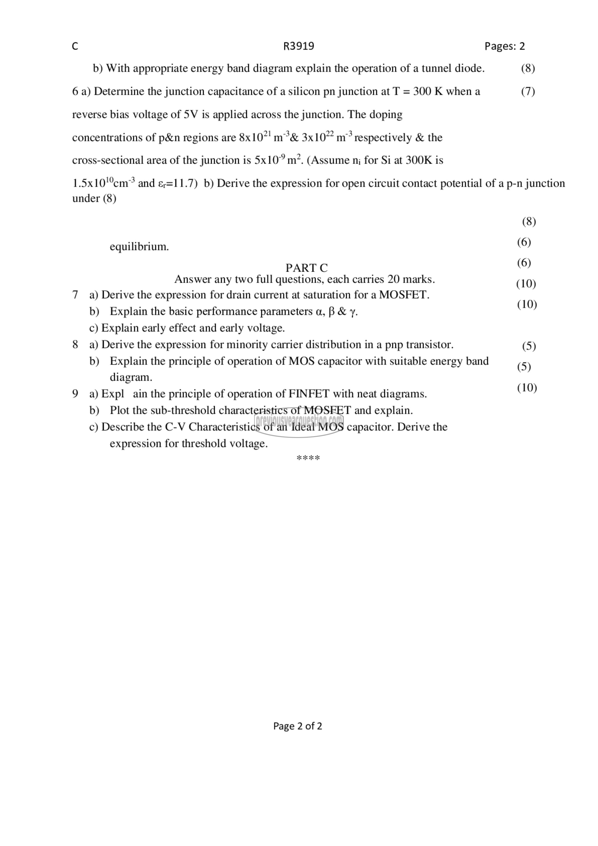
b) With appropriate energy band diagram explain the operation of a tunnel diode. (8)
6 a) Determine the junction capacitance of ೩ silicon pn junction at ಎ 300 K when a (7)
reverse bias voltage of 517 is applied across the junction. The doping
concentrations of p&n regions are 85107 m?& 3x10” जा respectively & the
cross-sectional area of the junction is 5%10 72. (Assume nj for Si at 300K is
1.5x10!cm* and ௨11.7) b) Derive the expression for open circuit contact potential of a p-n junction
under (8)
(8)
equilibrium. (6)
PART ¢ (6)
Answer any two full questions, each carries 20 marks. (10)
7 a) Derive the expression for drain current at saturation fora MOSFET.
b) Explain the basic performance parameters 0, B ൭൮. (10)
c) Explain early effect and early voltage.
8 a) Derive the expression for minority carrier distribution in a pnp transistor. (5)
b) Explain the principle of operation of MOS capacitor with suitable energy band (5)
diagram.
(10)
9 a) Expl ain the principle of operation of FINFET with neat diagrams.
b) Plot the sub-threshold characteristics of MOSFET and explain.
c) Describe the C-V Characteristics of an Ideal MOS capacitor. Derive the
expression for threshold voltage.
Page 2 of 2
