APJ ABDUL KALAM TECHNOLOGICAL UNIVERSITY Previous Years Question Paper & Answer
Semester : SEMESTER 8
Subject : Nano electronics
Year : 2019
Term : MAY
Scheme : 2015 Full Time
Course Code : EC 402
Page:1
Reg No.:_ Name:
Max. Marks: 100
b)
b)
b)
b)
b)
b)
b)
0)
111071 Pages: 2
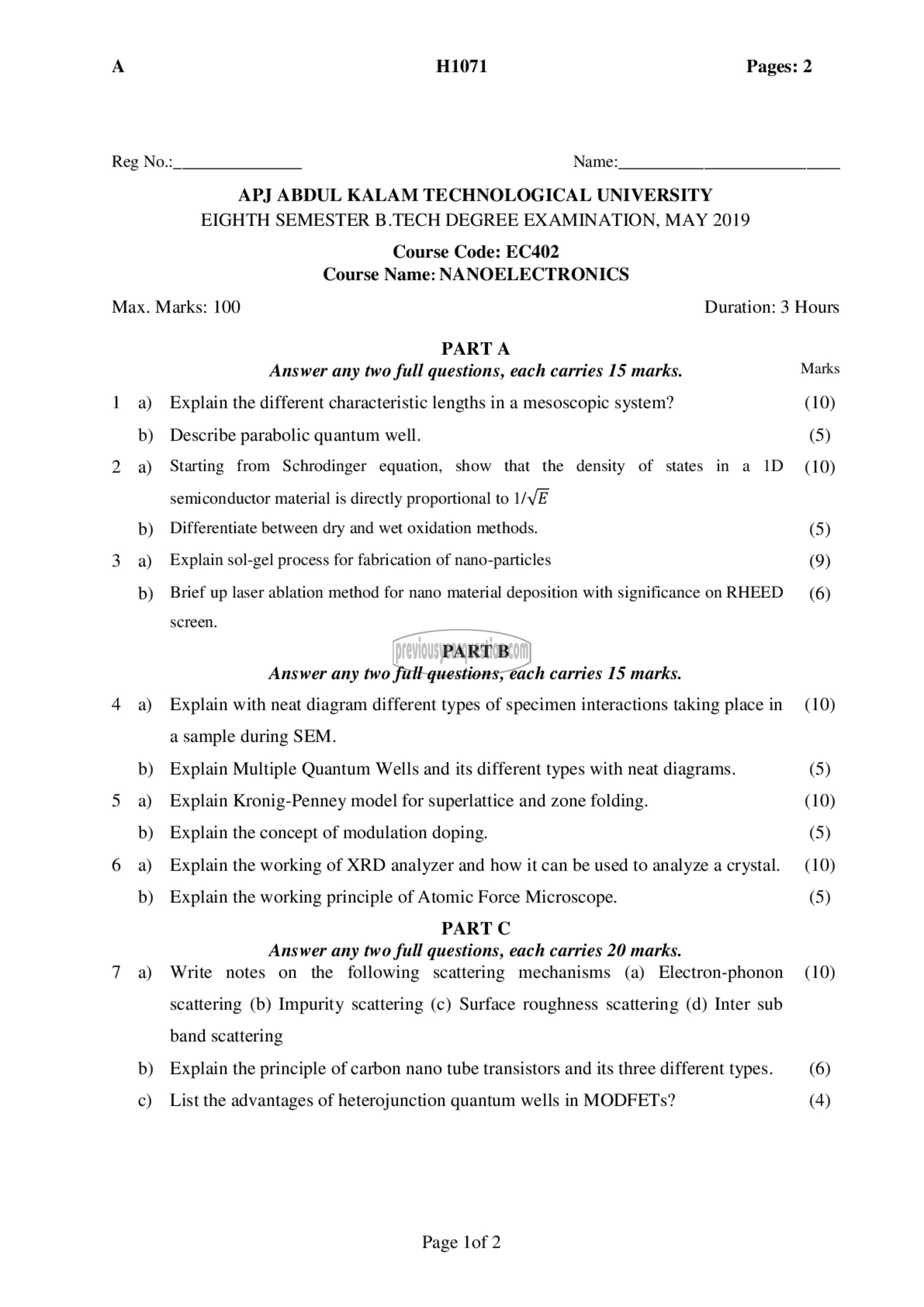
APJ ABDUL KALAM TECHNOLOGICAL UNIVERSITY
EIGHTH SEMESTER B.TECH DEGREE EXAMINATION, MAY 2019
Course Code: EC402
Course Name: NANOELECTRONICS
PARTA
Answer any two full questions, each carries 15 marks.
Explain the different characteristic lengths in a mesoscopic system?
Describe parabolic quantum well.
Starting from Schrodinger equation, show that the density of states in a 1D
semiconductor material is directly proportional to 1/۷۳
Differentiate between dry and wet oxidation methods.
Explain sol-gel process for fabrication of nano-particles
Brief up laser ablation method for nano material deposition with significance on RHEED
screen.
PART تا
Answer any two full questions, each carries 15 marks.
Explain with neat diagram different types of specimen interactions taking place in
a sample during SEM.
Explain Multiple Quantum Wells and its different types with neat diagrams.
Explain Kronig-Penney model for superlattice and zone folding.
Explain the concept of modulation doping.
Explain the working of XRD analyzer and how it can be used to analyze a crystal.
Explain the working principle of Atomic Force Microscope.
PART ட
Answer any two full questions, each carries 20 marks.
Write notes on the following scattering mechanisms (a) Electron-phonon
scattering (b) Impurity scattering (c) Surface roughness scattering (d) Inter sub
band scattering
Explain the principle of carbon nano tube transistors and its three different types.
List the advantages of heterojunction quantum wells in MODFETs?
Page lof 2
Duration: 3 Hours
Marks
(10)
(5)
(10)
(5)
(9)
(6)
(10)
(5)
(10)
(5)
(10)
(5)
(10)
(6)
(4)
