APJ ABDUL KALAM TECHNOLOGICAL UNIVERSITY Previous Years Question Paper & Answer
Semester : SEMESTER 3
Subject : Digital System Design
Year : 2020
Term : DECEMBER
Branch : INFORMATION TECHNOLOGY
Scheme : 2015 Full Time
Course Code : IT 201
Page:2
b)
0)
a)
b)
a)
b)
0)
a)
b)
0)
a)
b)
0)
020001T201092001
Implement a full adder using two 4 x 1 MUX (5)
Design a T flipflop from SR flipflop. (6)
What is an Excitation table? Give the excitation table of SR, JK, D and T flip (5)
flops.
Design the sequential circuit described by the following state equations. Use JK (10)
flip-flops.
A(t+1) = xAB + yA'C + xy
B(t+1) =xAC + ४5८"
C(t+1) = > + yAB’
PART C
Answer any two full questions, each carries 20 marks.
Give the circuit diagram of Universal Shift Register. Explain its capabilities. (7)
Design a Decade ripple counter using J-K Flipflop and explain it with the help (10)
of state diagram and timing diagram.
Discuss about the effect of propagation delay in clock period of ripple counters. (3)
Design a counter with binary count sequence 1-2-3-5-6-1. Use J-K flip flop to (6)
implement the counter.
Design a 4-bit Ring Counter using D flip flop. (4)
Explain Hamming Code? Explain its error detection operation for the data word (10)
“1100101077?
Draw and explain the logic diagram of a memory cell for storing one bit of (5)
information.
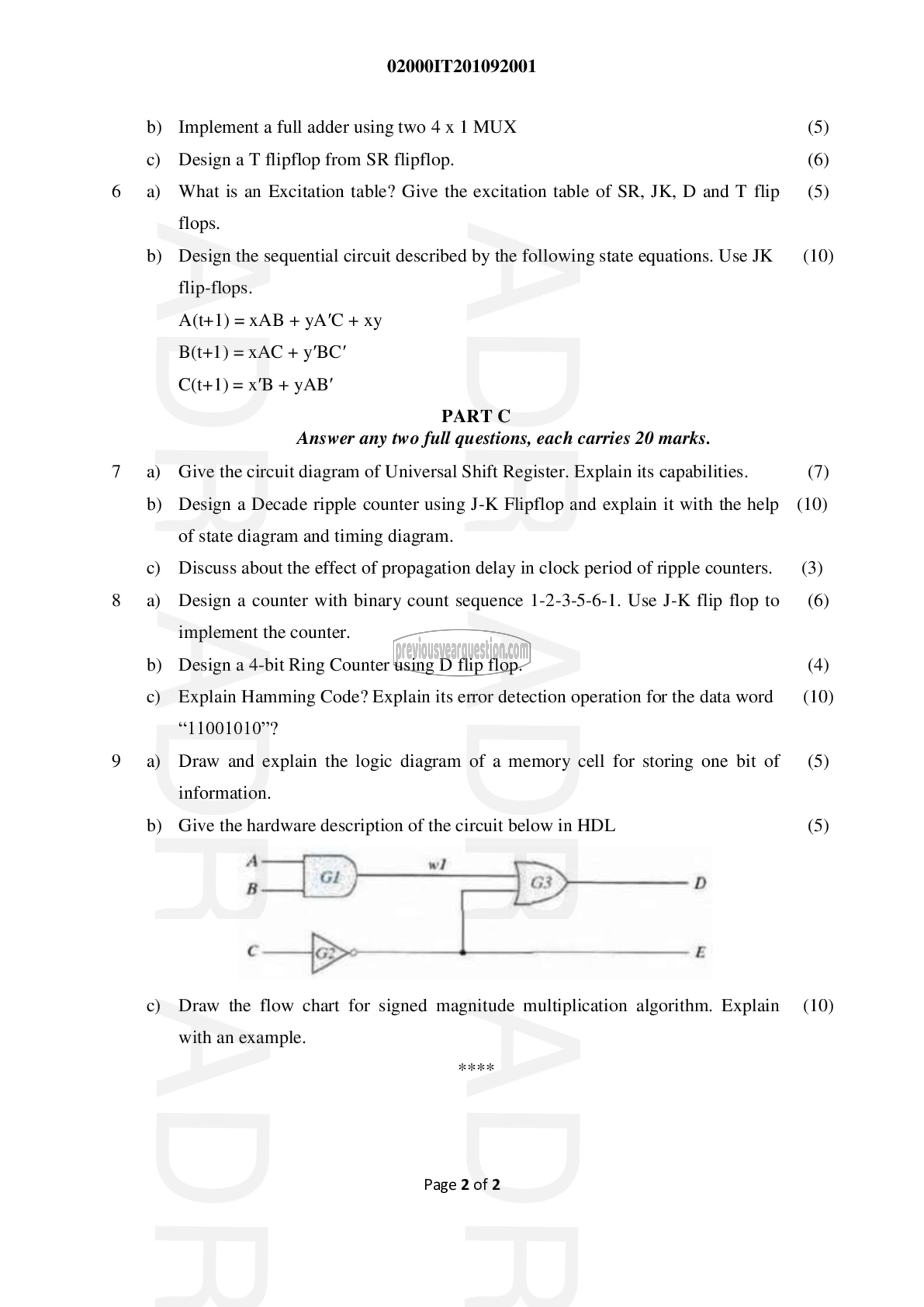
Give the hardware description of the circuit below in HDL (5)
A [ഫി
ப்
B By
Draw the flow chart for signed magnitude multiplication algorithm. Explain (10)
with an example.
Page 2 of 2
