APJ ABDUL KALAM TECHNOLOGICAL UNIVERSITY Previous Years Question Paper & Answer
Semester : SEMESTER 3
Subject : Switching Theory and Logic Design
Year : 2020
Term : DECEMBER
Branch : COMPUTER SCIENCE AND ENGINEERING
Scheme : 2015 Full Time
Course Code : CS 203
Page:2
12
13
14
15
16
17
a)
a)
b)
a)
b)
a)
a)
a)
b)
a)
b)
02000CS203092001
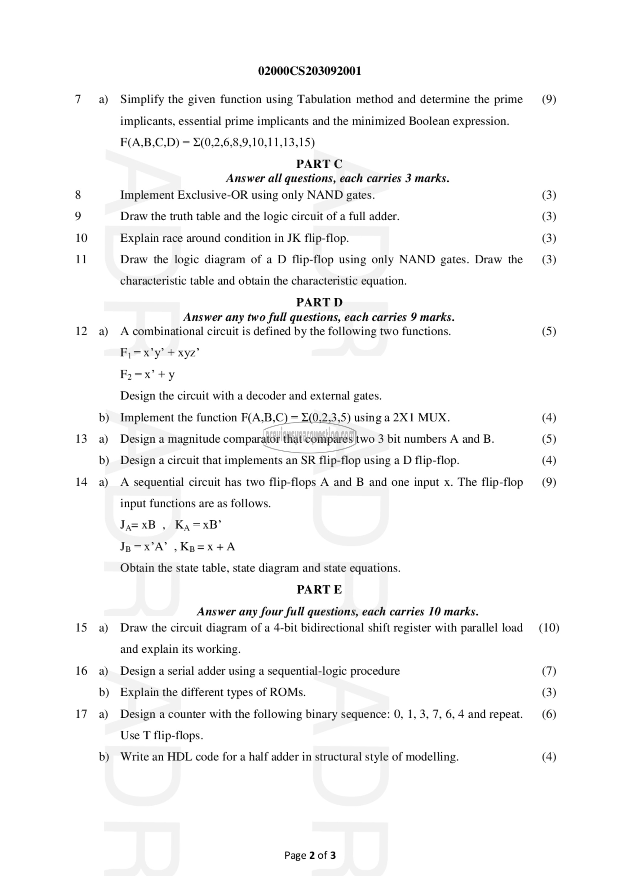
Simplify the given function using Tabulation method and determine the prime
implicants, essential prime implicants and the minimized Boolean expression.
F(A,B,C,D) = ೫(0,2,6,8,9,10,11,13,15)
PART C
Answer all questions, each carries 3 marks.
Implement Exclusive-OR using only NAND gates.
Draw the truth table and the logic circuit of a full adder.
Explain race around condition in JK flip-flop.
Draw the logic diagram of a D flip-flop using only NAND gates. Draw the
characteristic table and obtain the characteristic equation.
PART D
Answer any two full questions, each carries 9 marks.
A combinational circuit is defined by the following two functions.
F,=x’y’ + xyz’
F,=x’+y
Design the circuit with a decoder and external gates.
Implement the function F(A,B,C) = ೫(0,2,3,5) using a 2X1 MUX.
Design a magnitude comparator that compares two 3 bit numbers A and B.
Design a circuit that implements an SR flip-flop using a D flip-flop.
A sequential circuit has two flip-flops A and B and one input x. The flip-flop
input functions are as follows.
7७-58 , Ky =xB’
ലാക് ,Kp=x+A
Obtain the state table, state diagram and state equations.
PART E
Answer any four full questions, each carries 10 marks.
Draw the circuit diagram of a 4-bit bidirectional shift register with parallel load
and explain its working.
Design a serial adder using a sequential-logic procedure
Explain the different types of ROMs.
Design a counter with the following binary sequence: 0, 1, 3, 7, 6, 4 and repeat.
Use T flip-flops.
Write an HDL code for a half adder in structural style of modelling.
Page 2 of 3
(9)
(3)
(3)
(3)
(3)
(5)
(4)
(5)
(4)
(9)
(10)
(7)
(3)
(6)
(4)
