APJ ABDUL KALAM TECHNOLOGICAL UNIVERSITY Previous Years Question Paper & Answer
Semester : SEMESTER 4
Subject : Analog Communication Engineering
Year : 2020
Term : SEPTEMBER
Scheme : 2015 Full Time
Course Code : EC 208
Page:1
02000EC208052004
Pages: 2
Reg No.: Name:
Max. Marks: 100
1 a)
b)
2 a)
b)
3 a)
b)
4 a)
b)
ട് ஐ
b)
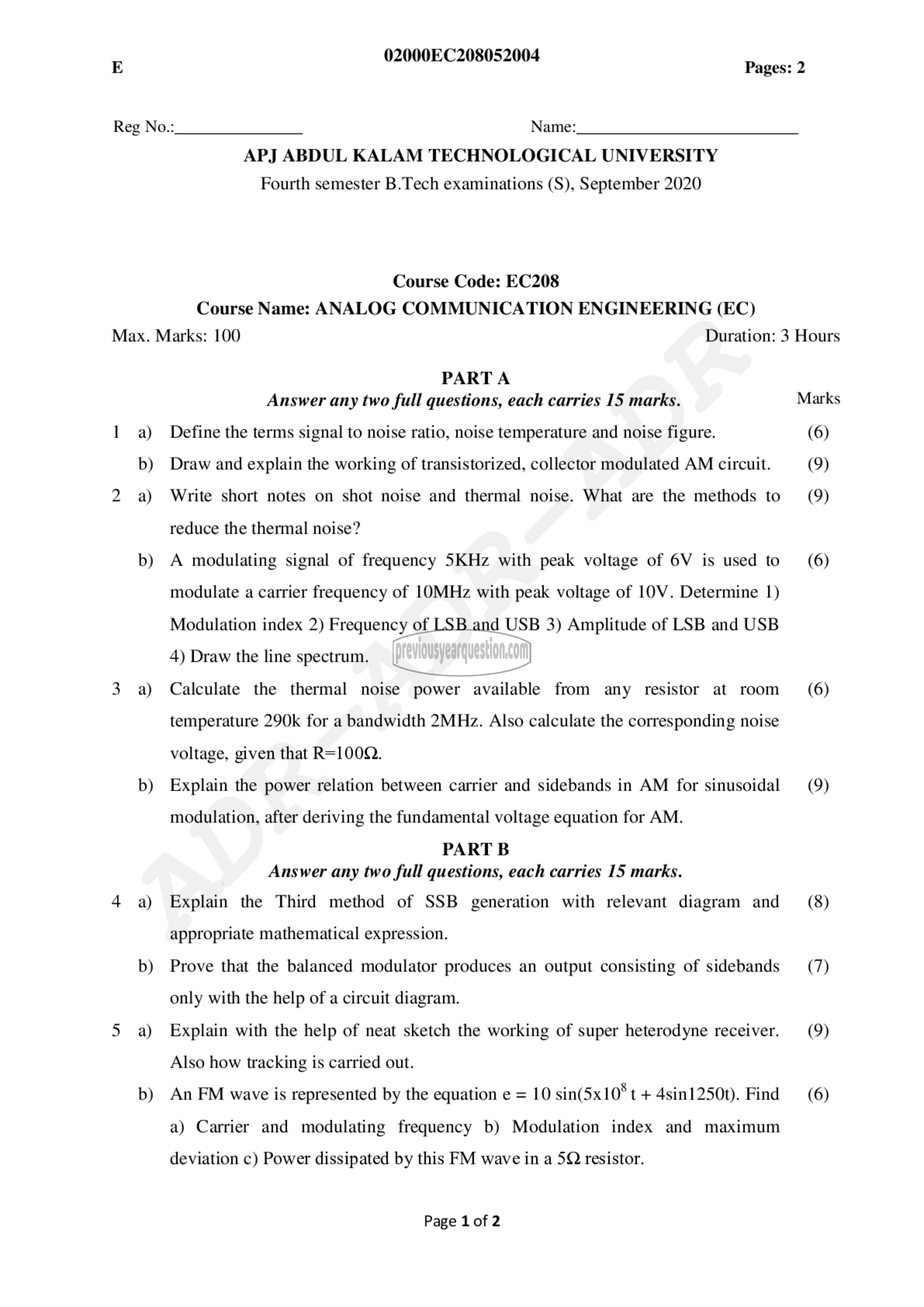
APJ ABDUL KALAM TECHNOLOGICAL UNIVERSITY
Fourth semester B.Tech examinations (S), September 2020
Course Code: EC208
Course Name: ANALOG COMMUNICATION ENGINEERING (EC)
PARTA
Answer any two full questions, each carries 15 marks.
Define the terms signal to noise ratio, noise temperature and noise figure.
Draw and explain the working of transistorized, collector modulated AM circuit.
Write short notes on shot noise and thermal noise. What are the methods to
reduce the thermal noise?
A modulating signal of frequency 5KHz with peak voltage of 6V is used to
modulate a carrier frequency of 101/1112 with peak voltage of 10V. Determine 1)
Modulation index 2) Frequency of LSB and USB 3) Amplitude of LSB and USB
4) Draw the line spectrum.
Calculate the thermal noise power available from any resistor at room
temperature 290k for a bandwidth 2MHz. Also calculate the corresponding noise
voltage, given that R=100Q.
Explain the power relation between carrier and sidebands in AM for sinusoidal
modulation, after deriving the fundamental voltage equation for AM.
PART 8
Answer any two full questions, each carries 15 marks.
Explain the Third method of SSB generation with relevant diagram and
appropriate mathematical expression.
Prove that the balanced modulator produces an output consisting of sidebands
only with the help of a circuit diagram.
Explain with the help of neat sketch the working of super heterodyne receiver.
Also how tracking is carried out.
An FM wave is represented by the equation € = 10 sin(5x10*t + 4sin1250t). Find
a) Carrier and modulating frequency b) Modulation index and maximum
deviation c) Power dissipated by this FM wave in a 5Q resistor.
Page 1 of 2
Duration: 3 Hours
Marks
(6)
(9)
(9)
(6)
(6)
(9)
(8)
(7)
(9)
(6)
