APJ ABDUL KALAM TECHNOLOGICAL UNIVERSITY Previous Years Question Paper & Answer
University : APJ ABDUL KALAM TECHNOLOGICAL UNIVERSITY
Course : B.Tech
Semester : SEMESTER 5
Subject : Digital System Design
Year : 2020
Term : SEPTEMBER
Scheme : 2015 Full Time
Course Code : EC 361
Page:3
PDF Text (Beta):
000008 0361121902
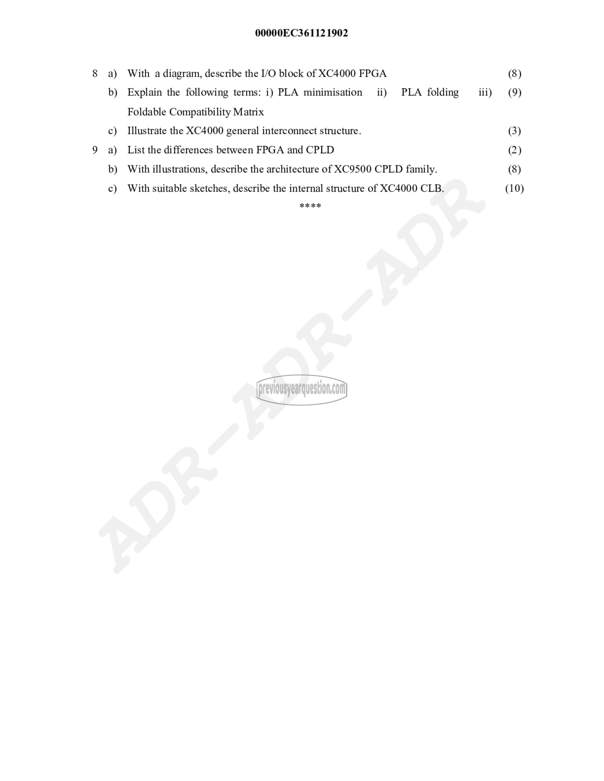
With a diagram, describe the I/O block of XC4000 FPGA
Explain the following terms: 1) PLA minimisation ii) PLA folding 111)
Foldable Compatibility Matrix
Illustrate the XC4000 general interconnect structure.
List the differences between FPGA and CPLD
With illustrations, describe the architecture of XC9500 CPLD family.
With suitable sketches, describe the internal structure of XC4000 CLB.
मे मर मै मे
(8)
(9)
(3)
(2)
(8)
(10)
Similar Question Papers
APJ ABDUL KALAM TECHNOLOGICAL UNIVERSITY =>
M.Tech =>
SEMESTER 1 =>
Advanced Digital Communication =>
2015 => DECEMBER =>
Download
APJ ABDUL KALAM TECHNOLOGICAL UNIVERSITY =>
M.Tech =>
SEMESTER 2 =>
Design Principles of power converters =>
2018 => MAY =>
Download
APJ ABDUL KALAM TECHNOLOGICAL UNIVERSITY =>
M.Tech =>
SEMESTER 2 =>
Antenna Theory and Design =>
2016 => MAY =>
Download
APJ ABDUL KALAM TECHNOLOGICAL UNIVERSITY =>
B.Tech =>
SEMESTER 7 =>
Chemical Engineering Design - II =>
2020 => DECEMBER =>
Download
APJ ABDUL KALAM TECHNOLOGICAL UNIVERSITY =>
B.Tech =>
SEMESTER 6 =>
Compiler Design =>
2020 => SEPTEMBER =>
Download
