APJ ABDUL KALAM TECHNOLOGICAL UNIVERSITY Previous Years Question Paper & Answer
Semester : SEMESTER 4
Subject : Digital Electronics and Logic Design
Year : 2019
Term : MAY
Scheme : 2015 Full Time
Course Code : EE 204
Page:2
12
13
14
15
16
a)
b)
a)
b)
a)
b)
a)
b)
D1034 Pages: 2
PART C
Answer any two questions, each carries 10 marks
Realise the Boolean expression F = ¥m(1,5,7,15) using a4 x 1 Multiplexer
Realise a full adder using two half adders.
Discuss the different types of shift registers.
Design a 3 bit asynchronous counter using JK flip flops.
What is a glitch? Show the timing diagram for a Mod 6 asynchronous counter
showing the glitches in the diagram.
How can a 2:4 decoder be used as 1:4 Demultiplexer?
PART 0
Answer any two questions, each carries 10 marks
Develop the logic circuit diagram and table for 4 -bit ring counter and explain
the working.
Explain the working of Flash type ADC.
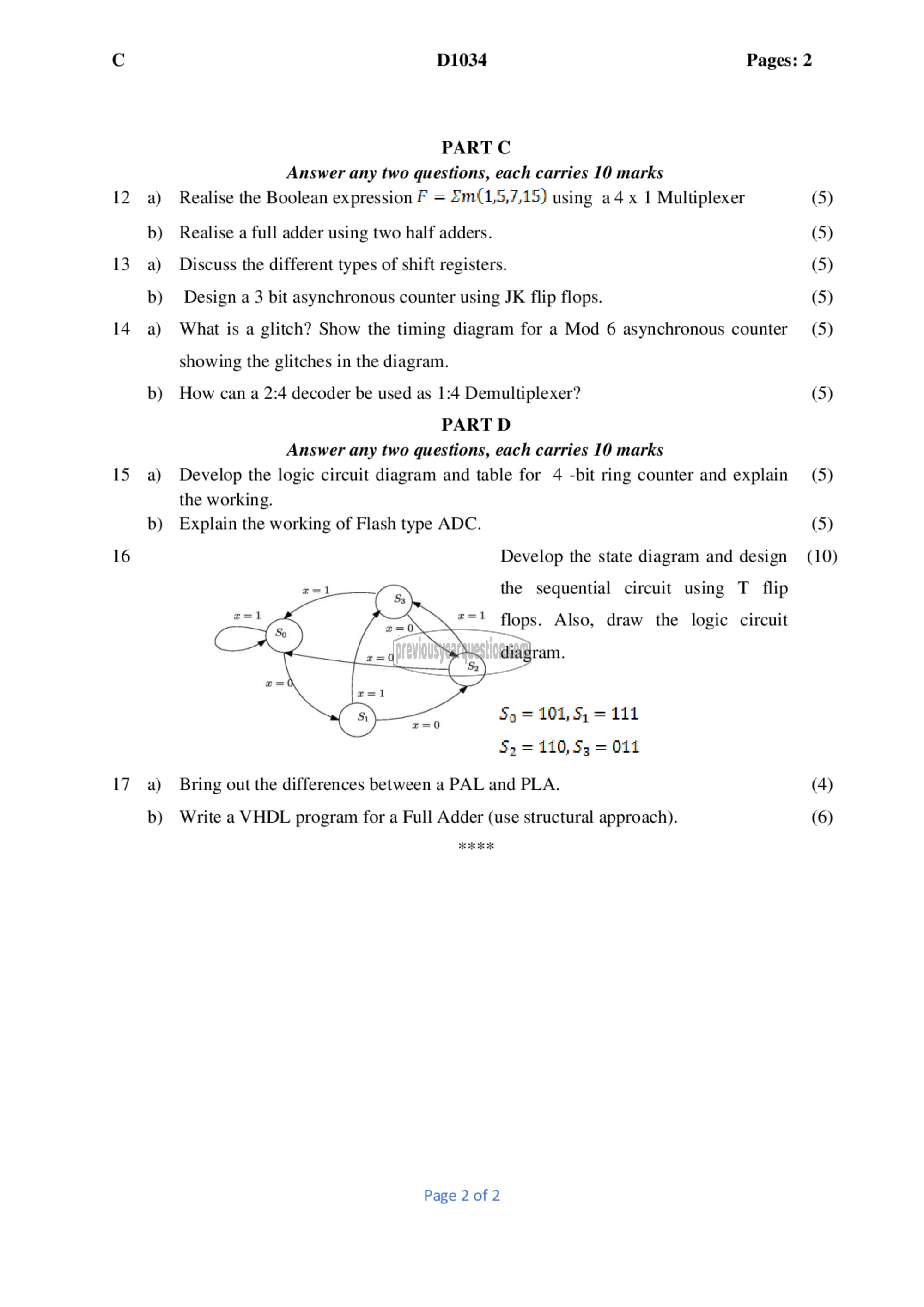
Develop the state diagram and design
the sequential circuit using T flip
flops. Also, draw the logic circuit
diagram.
111 = 51 ,101 = 50
011 = و5 ,110 = 52
17 ൮ Bring out the differences between ೩ PAL and PLA.
b)
Write a VHDL program for a Full Adder (use structural approach).
RE
Page 2 of 2
(5)
(5)
(5)
(5)
(5)
(5)
(5)
(5)
(10)
(4)
(6)
