APJ ABDUL KALAM TECHNOLOGICAL UNIVERSITY Previous Years Question Paper & Answer
Semester : SEMESTER 1
Subject : Power Converter Circuits
Year : 2017
Term : DECEMBER
Branch : POWER CONTROL AND DRIVES
Scheme : 2015 Full Time
Course Code : 01 EE 6501
Page:2
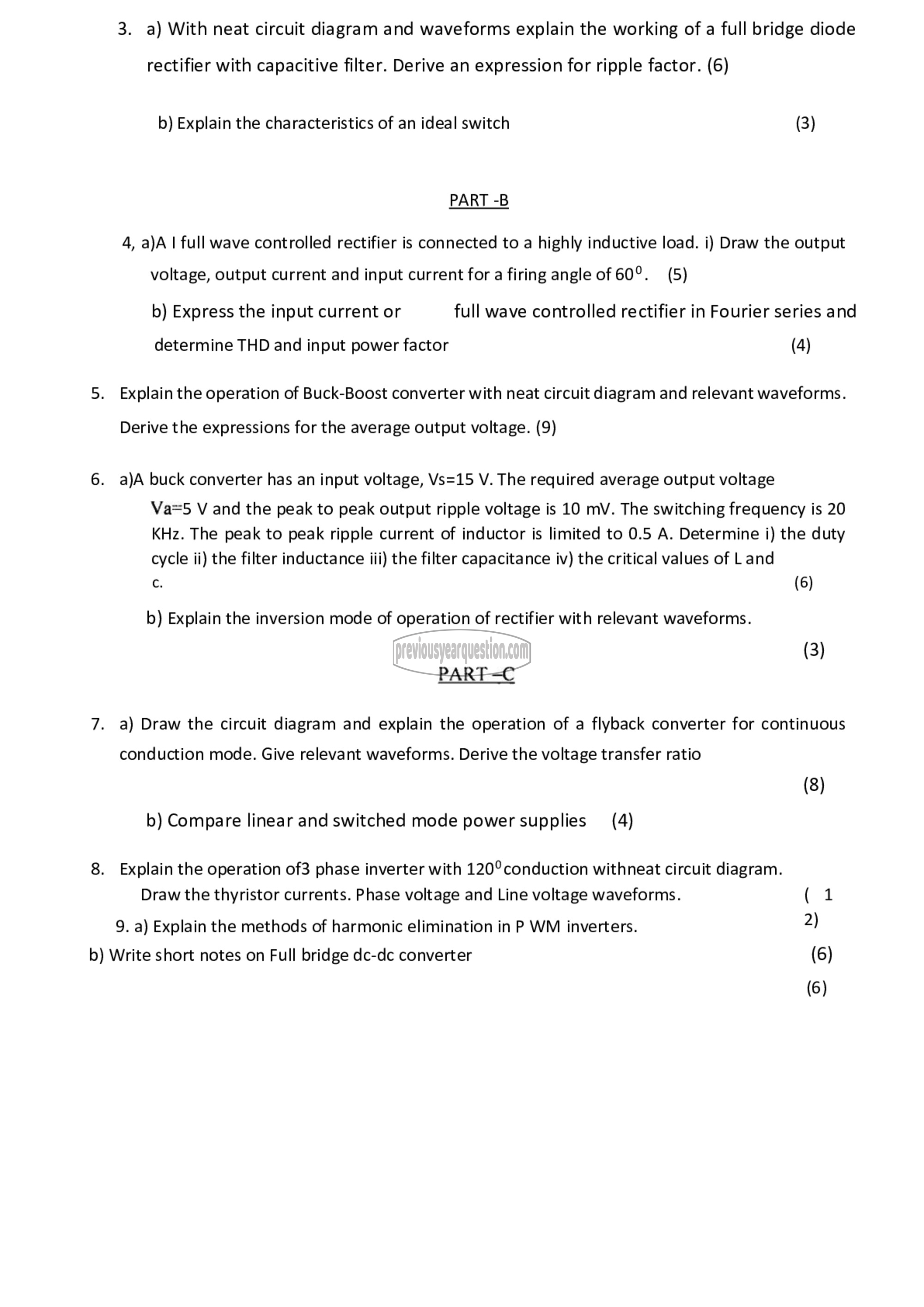
3. a) With neat circuit diagram and waveforms explain the working of a full bridge diode
rectifier with capacitive filter. Derive an expression for ripple factor. (6)
b) Explain the characteristics of an ideal switch
(3)
PART -B
4, a)A | full wave controlled rectifier is connected to a highly inductive load. i) Draw the output
voltage, output current and input current for a firing angle of 60°. (5)
b) Express the input current or full wave controlled rectifier in Fourier series and
(4)
determine THD and input power factor
5. Explain the operation of Buck-Boost converter with neat circuit diagram and relevant waveforms
Derive the expressions for the average output voltage. (9)
6. a)A buck converter has an input voltage, Vs=15 V. The required average output voltage
Va=5 V and the peak to peak output ripple voltage is 10 mV. The switching frequency is 20
KHz. The peak to peak ripple current of inductor is limited to 0.5 A. Determine i) the duty
cycle ii) the filter inductance iii) the filter capacitance iv) the critical values of Land
6
(6)
b) Explain the inversion mode of operation of rectifier with relevant waveforms.
(3)
PART -C
7. a) Draw the circuit diagram and explain the operation of a flyback converter for continuous
conduction mode. Give relevant waveforms. Derive the voltage transfer ratio
(8)
b) Compare linear and switched mode power supplies (4)
8. Explain the operation of3 phase inverter with 120°conduction withneat circuit diagram.
Draw the thyristor currents. Phase voltage and Line voltage waveforms. ( 1
9. a) Explain the methods of harmonic elimination in P WM inverters. 2)
b) Write short notes on Full bridge dc-dc converter (6)
(6)
