APJ ABDUL KALAM TECHNOLOGICAL UNIVERSITY Previous Years Question Paper & Answer
Semester : SEMESTER 1
Subject : Power Converter Circuits
Year : 2015
Term : DECEMBER
Branch : POWER CONTROL AND DRIVES
Scheme : 2015 Full Time
Course Code : 01 EE 6501
Page:1
APJ ABDUL KALAM TECHNOLOGICAL UNIVERSITY
FIRST SEMESTER M.TECH DEGREE EXAMINATION, DECEMBER 2015
ELECTRICAL & ELECTRONICS ENGINEERING
Stream: POWER CONTROL AND DRIVES
OIEE6501: POWER CONVERTER CIRCUITS
Time: 3 hours Max marks: 60
Answer any two full questions from each part. PART-A
(Module 1 and 11)
1 a. Derive an expression for average output voltage of a three phase diode (5)
rectifier with source inductance.
b. Determine the performance parameters of a single phase full wave diode (4) bridge
rectifier with R load.
2 a. (6)
With neat circuit diagram and waveforms explain the working of a full bridge diode
rectifier with capacitive filter. Derive an expression for ripple factor.
b. Explain Line Current Distortion (3)
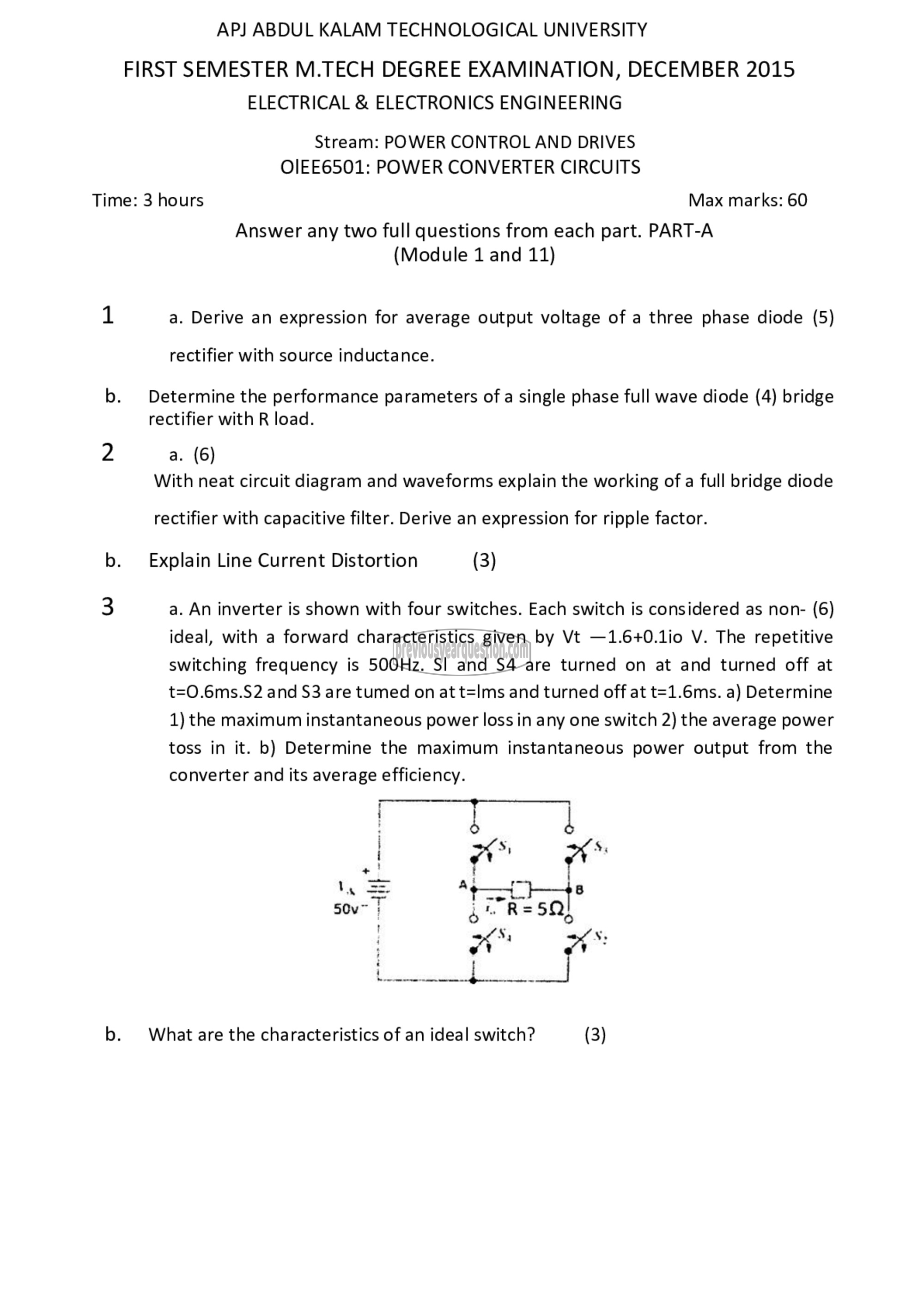
3 a. An inverter is shown with four switches. Each switch is considered as non- (6)
ideal, with a forward characteristics given by Vt —1.6+0.1io ४. The repetitive
switching frequency 15 500112. اك and 54 are turned on at and turned off at
t=0.6ms.S2 and 53 are tumed on at t=Ims and turned off at t=1.6ms. a) Determine
1) the maximum instantaneous power loss in any one switch 2) the average power
toss in it. b) Determine the maximum instantaneous power output from the
converter and its average efficiency.
| 5
। 1 ١
+ 1
1५ उड़ டர 4 த ப
5097 | ڑا =5Q)
b. What are the characteristics of an ideal switch? (3)
