APJ ABDUL KALAM TECHNOLOGICAL UNIVERSITY Previous Years Question Paper & Answer
Semester : SEMESTER 2
Subject : Design of VLSI Systems
Year : 2016
Term : MAY
Scheme : 2015 Full Time
Course Code : 01 EC 6122
Page:1
APJ ABDUL KALAM TECHNOLOGICAL
SECOND SEMESTER M.TECH DEGREE EXAMINATION, MAY 2016
Electronics & Communication
OIEC6122 Design of VLSI Systems
Max. Marks : 60 Duration: 3 Hours
Instruction: Answer any two questions from each module.
PART A
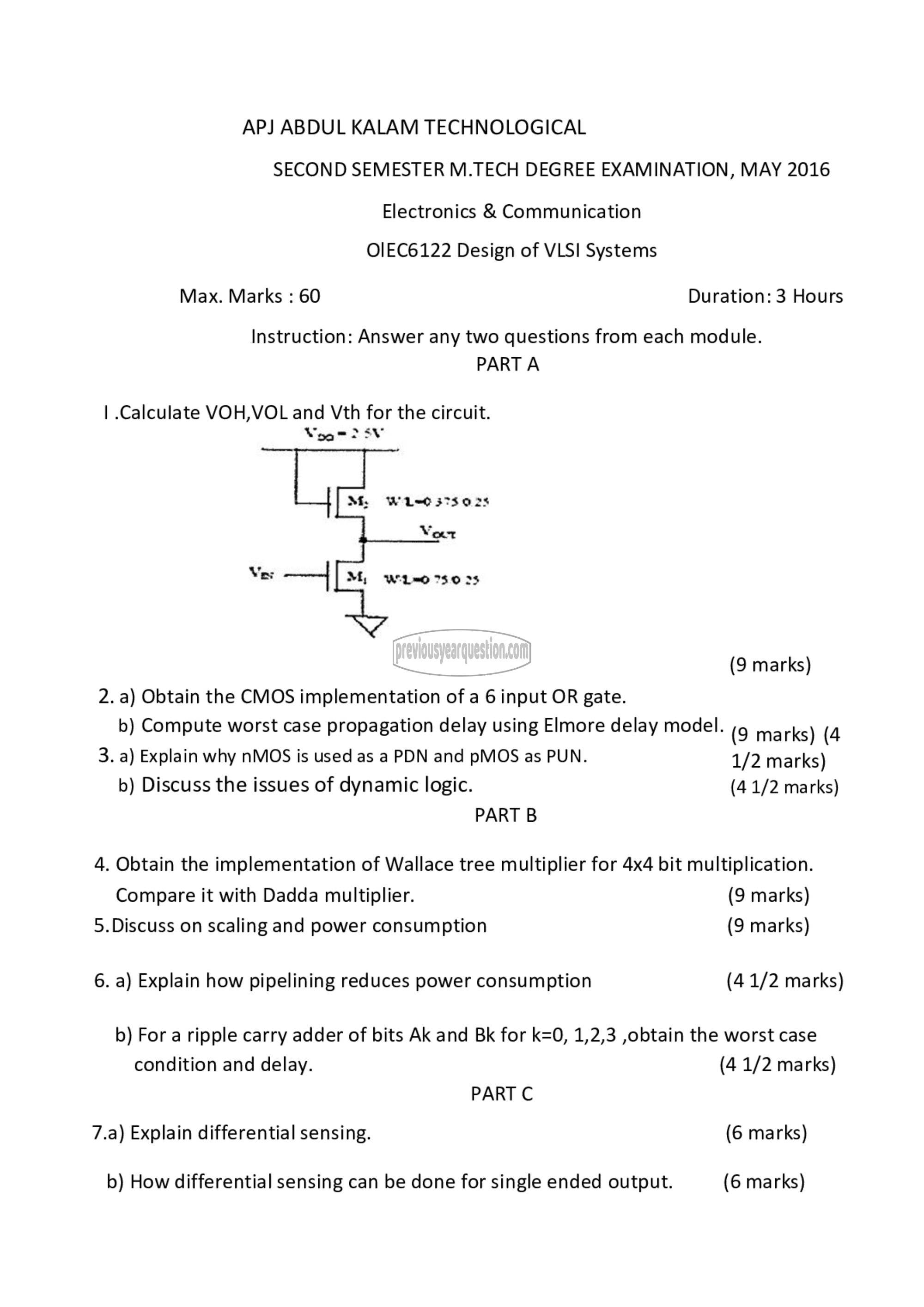
| .Calculate VOH,VOL and Vth for the circuit.
Von ಇ 2 5९९
= 1.०० 375 025
Voor
My, ६३०७० 75.0 25
(9 marks)
2. a) Obtain the CMOS implementation of a 6 input OR gate.
b) Compute worst case propagation delay using Elmore delay model. (9 marks) (4
3. a) Explain why nMOS is used as a PDN and pMOS as PUN. 1/2 marks)
b) Discuss the issues of dynamic logic. (4 1/2 marks)
PART B
4. Obtain the implementation of Wallace tree multiplier for 4x4 bit multiplication.
Compare it with Dadda multiplier. (9 marks)
5.Discuss on scaling and power consumption (9 marks)
6. a) Explain how pipelining reduces power consumption (4 1/2 marks)
0) For a ripple carry adder of bits Ak and Bk for k=0, 1,2,3 ,obtain the worst case
condition and delay. (4 1/2 marks)
PART C
7.a) Explain differential sensing. (6 marks)
b) How differential sensing can be done for single ended output. (6 marks)
