APJ ABDUL KALAM TECHNOLOGICAL UNIVERSITY Previous Years Question Paper & Answer
Semester : SEMESTER 3
Subject : Solid State Devices
Year : 2018
Term : DECEMBER
Scheme : 2015 Full Time
Course Code : EC 203
Page:1
6 R3919 Pages: 2
Reg No.: Name:
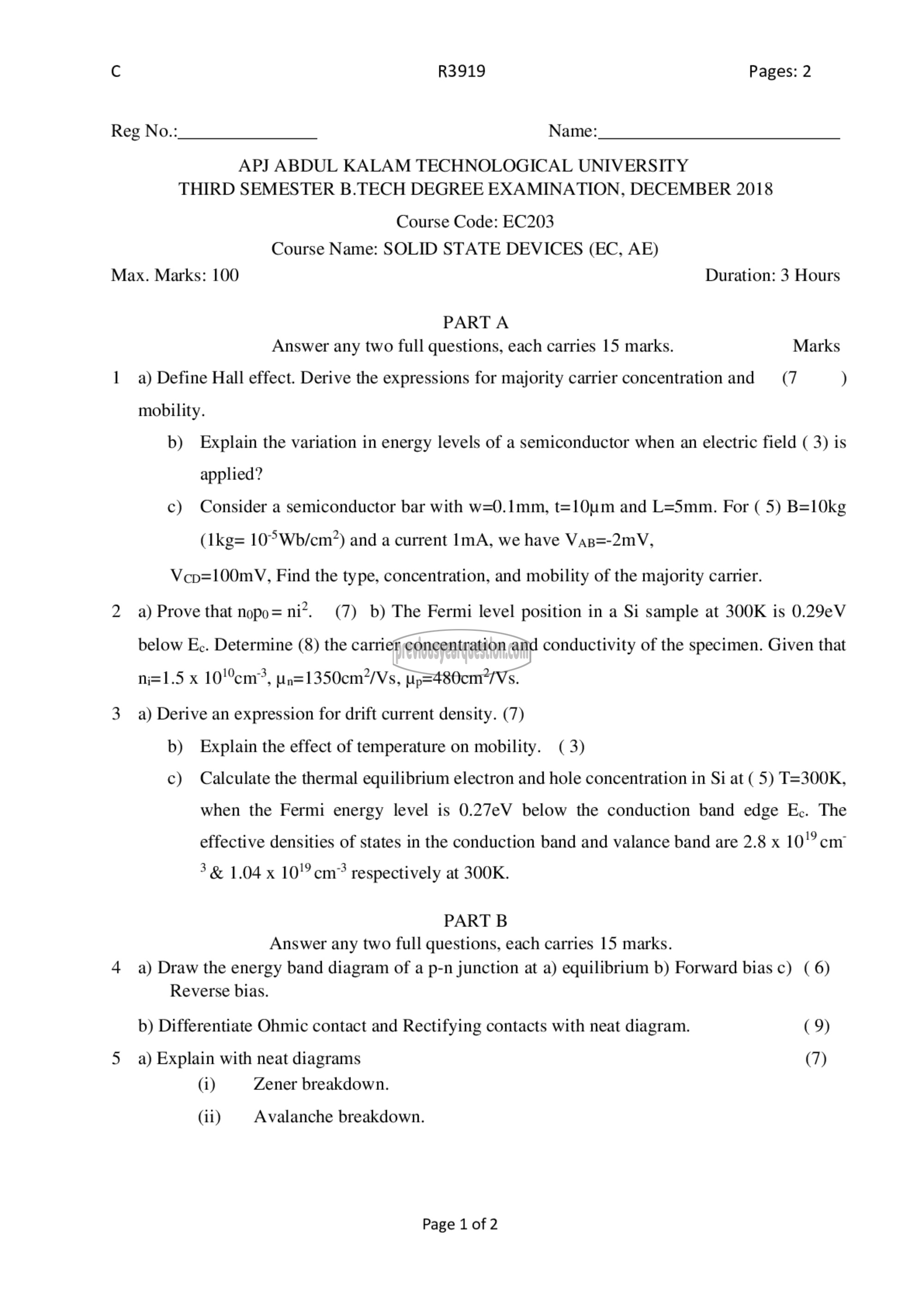
APJ ABDUL KALAM TECHNOLOGICAL UNIVERSITY
THIRD SEMESTER B.TECH DEGREE EXAMINATION, DECEMBER 2018
Course Code: EC203
Course Name: SOLID STATE DEVICES (EC, AE)
Max. Marks: 100 Duration: 3 Hours
PART A
Answer any two full questions, each carries 15 marks. Marks
1 a) Define Hall effect. Derive the expressions for majority carrier concentration and (7 )
mobility.
b) Explain the variation in energy levels of a semiconductor when an electric field ( 3) is
applied?
€) Consider a semiconductor bar with w=0.1mm, t=!10um and L=S5mm. For ( 5) B=10kg
(110ಎ 10°Wb/cm?) and a current ImA, we have Vap=-2mV,
Vcp=100mV, Find the type, concentration, and mobility of the majority carrier.
2 a) Prove that nopo= 7112. (7) b) The Fermi level position in a Si sample at 300K is 0.29eV
below Ec. Determine (8) the carrier concentration and conductivity of the specimen. Given that
اعم 5 x 10!cm, un=1350cm7/Vs, Up=480cm7/Vs.
a) Derive an expression for drift current density. (7)
b) Explain the effect of temperature on mobility. (3)
c) Calculate the thermal equilibrium electron and hole concentration in Si at (5) T=300K,
when the Fermi energy level is 0.27eV below the conduction band edge Ec. The
effective densities of states in the conduction band and valance band are 2.8 x 1017 cm
3 & 1.04 x 10⁷? ला उ respectively at 300K.
PART B
Answer any two full questions, each carries 15 marks.
4 a) Draw the energy band diagram of ೩ p-n junction at a) equilibrium b) Forward bias 0) ( 6)
Reverse bias.
b) Differentiate Ohmic contact and Rectifying contacts with neat diagram. (9)
5 a) Explain with neat diagrams (7)
(i) Zener breakdown.
(ii) Avalanche breakdown.
Page 1 of 2
