APJ ABDUL KALAM TECHNOLOGICAL UNIVERSITY Previous Years Question Paper & Answer
Semester : S1 and S2
Subject : INTRODUCTION TO ELECTRONICS ENGINEERING
Year : 2018
Term : APRIL
Branch : MECHANICAL ENGINEERING
Scheme : 2015 Full Time
Course Code : BE 101-04
Page:2
D
14 a)
b)
15 ஐ
0)
16 a)
0)
17 a)
0)
18 a)
0)
19 a)
0)
20 a)
0)
21804 Pages: 2
OR
Draw and explain the circuit of a common emitter RC coupled amplifier using
NPN transistorwith voltage divider biasing.
Draw the frequency response of a RC coupled amplifier and explain how gain
reduces at low and high frequencies.
Module IV
Draw the Vps v/s Ip curve of an enhancement MOSFET and mark different operating
regions.
With help of neat sketches, explain how an increase in Vps affects channel field and
drain current ina MOSFET.
OR
Draw the structure of N channel depletion MOSFET.
Explain the working of a depletion mode MOSFET.
Module V
Draw the circuit of a full wave bridge rectifier and derive the equations for
Vims, ೫60 and ripple factor.
Explain the term rectifier efficiency.
OR
Draw the block diagram of a DC power supply and explain the working of each stage.
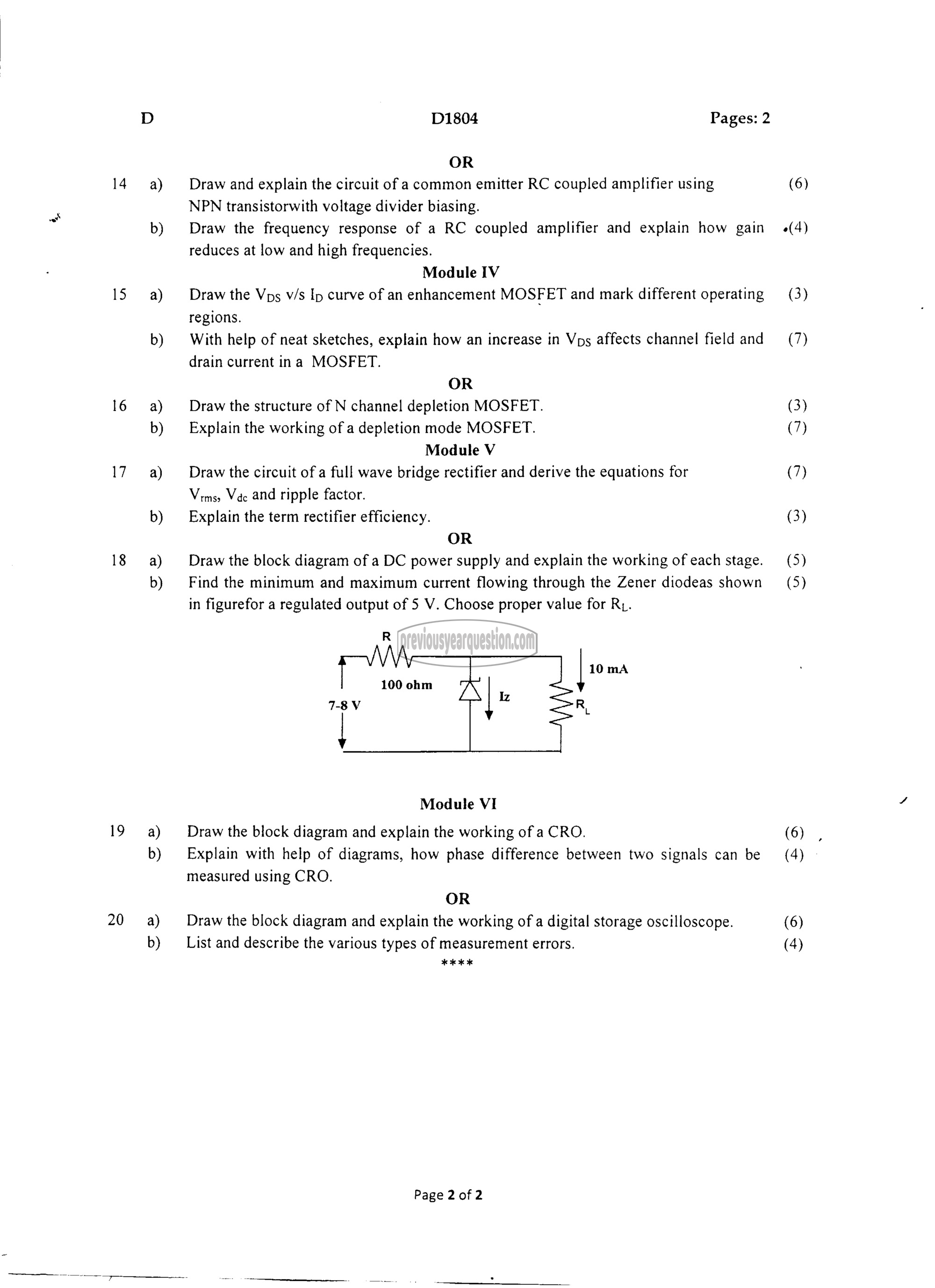
Find the minimum and maximum current flowing through the Zener diodeas shown
in figurefor a regulated output of 5 V. Choose proper value for Ri.
R
R
7-89 1
10 mA
100 ohm 02 ۱ 5
Module VI
Draw the block diagram and explain the working of a CRO.
Explain with help of diagrams, how phase difference between two signals can be
measured using CRO.
OR
Draw the block diagram and explain the working of a digital storage oscilloscope.
List and describe the various types of measurement errors.
اد ہد ಹ ೫%
Page 2 of 2
(6)
(4)
(3)
(7)
(3)
(7)
(7)
(3)
(5)
(5)
(6)
(4)
(6)
(4)
