APJ ABDUL KALAM TECHNOLOGICAL UNIVERSITY Previous Years Question Paper & Answer
Semester : S1 and S2
Subject : INTRODUCTION TO ELECTRONICS ENGINEERING
Year : 2017
Term : DECEMBER
Branch : MECHANICAL ENGINEERING
Scheme : 2015 Full Time
Course Code : BE 101-04
Page:2
14
15
18
19
20
a)
b)
a)
b)
a)
a)
b)
D7083
Draw the piece-wise linear model of diode and explain. (5)
Module III
Explain the output characteristics of transistor in CE configuration and 3 regions (5)
of operation.
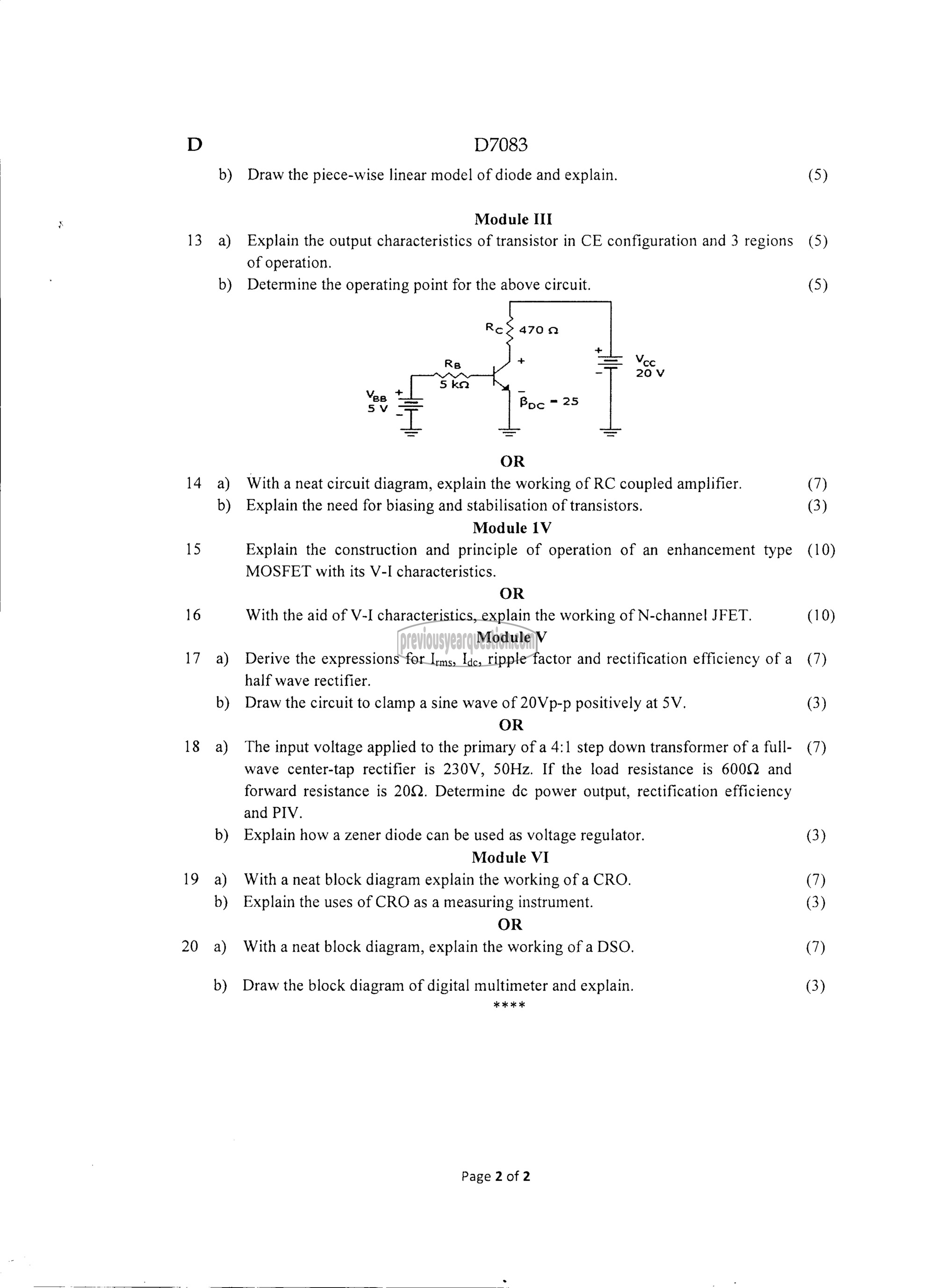
Determine the operating point for the above circuit. (5)
OR
With a neat circuit diagram, explain the working of RC coupled amplifier. (7)
Explain the need for biasing and stabilisation of transistors. (3)
Module 1V
Explain the construction and principle of operation of an enhancement type (10)
MOSFET with its V-I characteristics.
OR
With the aid of V-I characteristics, explain the working of N-channel JFET. (10)
Module V
Derive the expressions for Irms, luc, ripple factor and rectification efficiency of a (7)
half wave rectifier.
Draw the circuit to clamp a sine wave of 20Vp-p positively at 5V. (3)
OR
The input voltage applied to the primary of a 4:1 step down transformer of a full- (7)
wave center-tap rectifier is 230V, 50Hz. If the load resistance is 600Q and
forward resistance is 20Q. Determine de power output, rectification efficiency
and PIV.
Explain how a zener diode can be used as voltage regulator. (3)
Module VI
With a neat block diagram explain the working of a CRO. (7)
Explain the uses of CRO as a measuring instrument. (3)
OR
With a neat block diagram, explain the working of a DSO. (7)
Draw the block diagram of digital multimeter and explain. (3)
%%%%
Page 2 of 2
